

KiCad Tutorial 1/5 – Getting Started with KiCad
We have already begun our deep dive into the world of PCB designing with our last article in which we learnt the Basics of PCB. As mentioned in that article, we will continue with our PCB designing journey by learning how to use PCB Design Software’s. In the same regard, this tutorial is the first part of a series of tutorials in which we will learn how to use KiCad software.
In this tutorial we will explore the origin of KiCad, why it was selected above the others, advantages, disadvantages and finally installing and getting around its interface.
Introduction to KiCad
KiCad (pronounced Key-Cad) is an open-source software suite containing series of software used in computer-aided electronics design. It was originally developed by Jean-Pierre Charras in 1992 to provide an open source free alternative to commercial EDA software at the time. It features an integrated environment for schematic capture and PCB layout design along with CAM features that give users the ability to obtain data like Gerber files and bill of materials which are required for manufacturing designs. It also possesses a 3D viewer for the PCB layout which until recently was not available in commercial/ premium EDA software like Eagle.
The main strength behind the development of KiCad is its open source nature. KiCad has over the years benefitted from several paid and "not-paid" volunteers all of which have contributed in one way or the other to help KiCad grow to a point where it can be said to be on par with several commercial EDA software. It is supported by the KiCad community where you can always find help whenever you get stuck on using the software or if in need of a custom part or footprint which usually someone in the community would have created.
KiCad being a suite of software as mentioned earlier contains a series of software, all of which are interconnected (Changes made in one could be made to reflect in the other) and perform key functions in the design of electronic circuits. These software include;
Advantages of KiCad There are several reasons why you should consider the use of KiCad for the design of your projects.
1. KiCad is free: Due to its open-source nature, KiCad is available for use free of charge under the GPL License. This makes it the ideal tool for small startups and individuals who may not be able to afford the cost of other commercial EDA software. Donations to support it are however accepted.
2. Mature: Open source or not, KiCad is generally considered as one of the most matured EDA software capable of being used for successful development and maintenance of complex electronics board.
3. No Limitations: Unlike most other EDA tools which put up one limitation or the other based on the kind of license you purchase, KiCad comes with no limitations. It has no board-size limitation and easily handles up to 32 copper layers, up to 14 technical layers and up to 4 auxiliary layers. It can create all the files necessary for the production of the designed circuit boards including the Gerber files for photo-plotters, drilling files, component location files and a lot more.
4. Large Community
As common with Open-Source Software, KiCad has a large community which makes regular updates to the software an easy task. The community members via the forum are also quick to respond to questions to help newcomers learn fast and contribute parts, footprints, etc which makes development easier and faster compared to other software.
5. Ideal for Open Source Projects
Being an open source (GPL licensed) software, KiCad represents the ideal tool for projects oriented towards the creation of electronic hardware with an open-source flavor.
Disadvantages of KiCad
KiCad comes as good as EDA software can be with all the necessary features all defined in its own way which may present a little bit of challenge to people who are used to working with other software. But like any language, as soon as the basics are acquired, you will feel right at home with KiCad. For users familiar with software like Proteus, they may be disappointed at the lack of simulation features present in Proteus, but this is a feature that is also absent in most other EDA software.
Installing KiCad
KiCad supports all the popular (GNU/Linux, Apple macOS, and Windows) operating systems, with some minor difference in the way the software are installed on them. Up to date installation instructions and download links can be found here. http://www.KiCad-pcb.org/download/
For stable build versions of KiCad on MacOS and Windows, it is usually as simple as downloading the installation executable/image and running it on your computer. You could also decide to download the KiCad source code and perform the compilation and installation on your PC.
Getting Started with KiCad
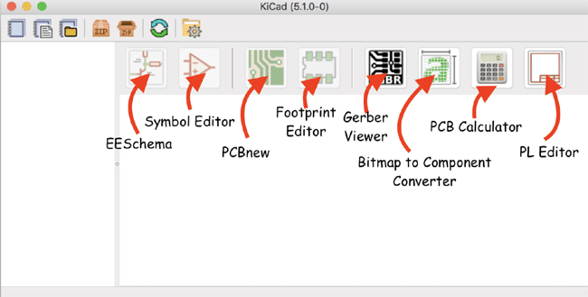
With the installation complete, launch the software. As mentioned in the introduction, KiCad as a suite contains a series of software used for EDA. The KiCad software package consists of
- KiCad Project Manager
- EEschema
- Pcbnew
- GerbView
- Bitmap2Component
- PCB Calculator
- PI Editor
Of these packages, three of them namely KiCad Project manager, EEschema, and PCBnew are at the core of every KiCad project. EEschema is the schematic creation tool in KiCad, it has features like linked hierarchical schematic sheets, custom symbol creation, and an ERC (electrical rules check). PCBnew, on the other hand, handles PCB design within KiCad. It is one of the most flexible PCB design software with features that allow developers create additional tools via the "new tool framework", augment their design with python scripts and verify their designs using its design rule checker (DRC). It also features high-speed PCB routing tools such as track-length matching and an interactive Autorouter, while also supporting external routing software like Top router and Free routing.
Interaction between these software is managed by the KiCad project manager. The files from all of the software used must be included to share a KiCad project without errors.
The table below shows the file extension of all the software.
|
S/N |
Program Name |
Description |
File Extension |
|
1. |
KiCad |
Project Manager |
*.pro |
|
2. |
Eeschema |
Schematic and Component Editor |
*.sch, *.lib, *.net |
|
3. |
PCBnew |
Circuit board and footprint editor |
*.KiCad_pcb, *.KiCad_mod |
|
4. |
GerbView |
Gerber and drill file viewer |
|
|
5. |
Bitmap2Component |
Convert bitmap images to components or footprints |
|
|
6. |
PCB Calculator |
Calculator for components, track width, electrical spacing, color codes, etc. |
|
|
7. |
PI Editor |
Page layout editor |
|
All of this software will be displayed in a project panel as shown below when you launch KiCad.
KiCad - Workflow
The KiCad Workflow is similar to that of other EDA software. Project starts with creating the schematics and from there the PCB is generated and finally Gerber files are created. Usually, this is a loop process as changes are sometimes required to be made to the schematics after the PCB has been created or the PCB, after the Gerber files have been created.
The design process is also usually punctuated with the need to create custom parts/footprints for components. All of this is properly detailed in the KiCad Workflow illustrated with a flowchart below.
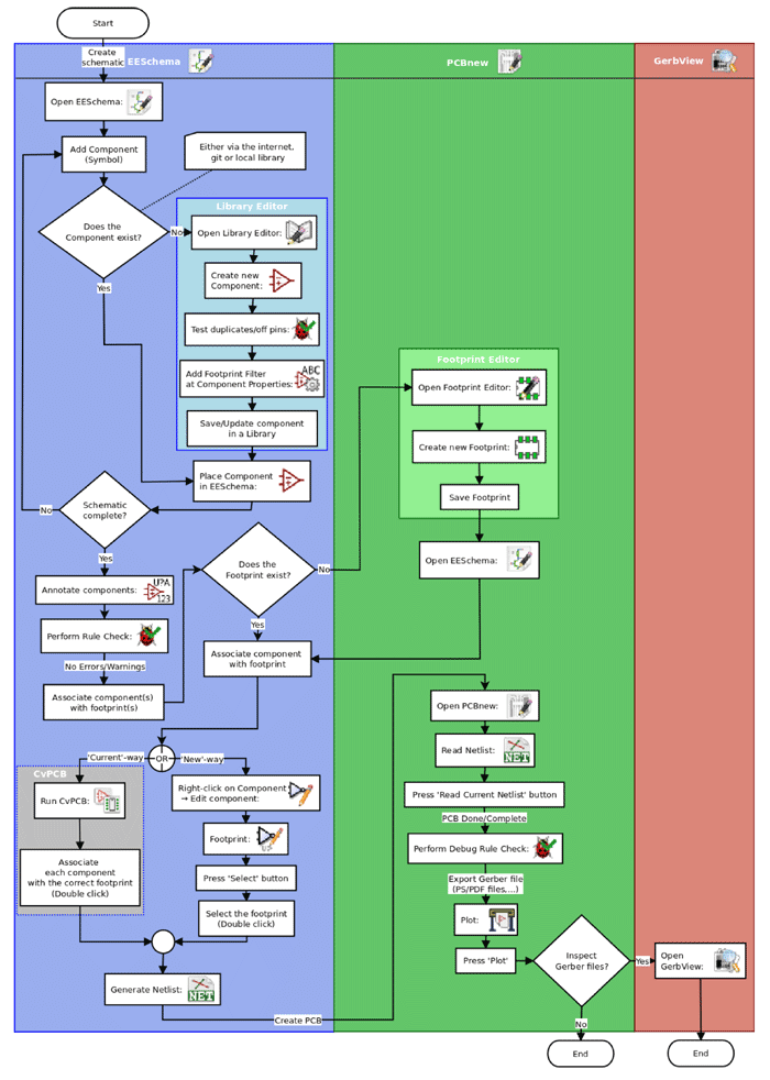
Despite its similarities with other PCB design software, the KiCad workflow distinguishes itself from other software in that Schematic symbols in Eeschema are very loosely coupled to footprints in PCBnew. For example, a single 0805 footprint can be used for capacitors, resistors, inductors, etc. As such, unlike other software, footprints are not selected during the creation of the schematics. This will be demonstrated in the third part of this series where we will develop a project example.
KiCad Shortcuts
KiCad like every other software has a series of keyboard shortcuts which can be used to increase the speed at which design actions are performed. These shortcuts are classified into two types in KiCad namely;
- Accelerator keys
- Hotkeys
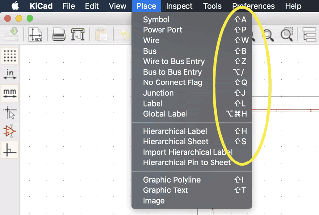
1. KiCad Accelerator keys
Accelerator keys work the same way as clicking on a menu or toolbar icon: the command will be entered but nothing will happen until the left mouse button is clicked. Accelerator keys are used when you want to enter a command mode without the need for immediate action. They are shown on the right side of menu panes so you know which combination of keys corresponds to a menu/toolbar icon.
2. KiCad Hotkeys
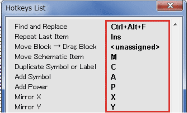
Hotkeys, on the other hand, are used for commands with immediate actions. Using a hotkey starts the command immediately at the current cursor location. It helps in the creation of a smooth workflow. A list of hotkeys available in KiCad can be accessed and modified (configure specific keys to specific actions) via Help → List Hotkeys or press Ctrl+F1.
For the next part of this tutorial, we will be looking at creating a new project on KiCad and designing your schematics in KiCad. We will be putting all of the shortcuts we learnt here to use and examine other features like creating hierarchical schematic sheets among others. So get your KiCad installed, ensure you install one of the latest updates so you will be able to follow my actions step by step. Thanks for reading. Do feel free to reach out via the comment section with questions, general comments, and notes about any section of PCB design you'd like me to cover specially.
Till Next time!

Latest Articles
-

Exploring the Different Types of PCB Layers and its Purpose
-

PCB Connectors: A Comprehensive Guide to the Different Types and Their Applications
-

PCB Soldering Steps
-

Basic Electronic Component Symbols that Every PCB Design Engineer Should Know
-

Home Made PCBs – A Step by Step guide to build PCBs in your Home
-

SMT Soldering Process in PCB Assembly Factory
Comments