

Printed Circuit Boards (PCBs) – Basics, Types, Terminologies and Design Tools
An average electronic circuit could consist of anywhere between tens to hundreds of components in it. While breadboards and dot boards might work for small circuits and design validations it is not practical to use them in final products or in larger circuit. In earlier times a method called wire wrapping was used by engineers to create permanent connections. In this method the leads of components were actually wrapped (coiled) with other leads to form connections. But as the circuits became complex they created a huge mess and occupied a lot of space in final products. This called for a new method which will be more reliable and compact for building electric connections between components.
Further as the silicon and integrated circuits became more popular in the 20th century, the size and cost of electronic components began to decrease and the demand in electronics products increased. At this point, due to the rise in demand, it no longer made sense to keep using old methods of manufacturing electronics like wire wrapping as they were time consuming and costly. This created a drive for a better solution which led to the development of the Printed Circuit Boards in the year 1936 by Pail Eishler. These Printed circuit boards are also called as Circuit Boards or PCB for short. In this article we will learn more about these PCB, their types, materials used in making them, and some basic terminologies and concepts associated with their design.
What is a PCB?
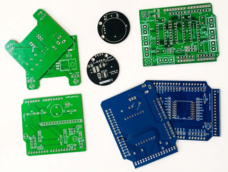
In today’s world Printed circuit boards have become very popular that it needs no introduction. Every one of us might have come across this green board at least once in our common electronic devices like remotes, Toys, alarm clocks etc. These Printed circuit boards mechanically support and electrically connect all electronic components in a circuit design using conductive tracks, pads and other features etched from one or more sheet layers of copper on a non-conductive substrate. Most times we take this humble board for granted and often pay no attention as to how it works. In this article we dig deep into these PCB and analyze them by each layer.
Layers of a PCB
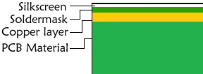
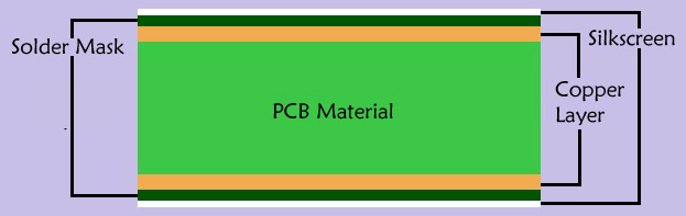
There are many types of PCB options available in the market today, but irrespective of the type, every Printed circuit board will be made up of the following layers. The layers are arranged from top to bottom or easy understanding. Further the image below illustrates each layer in a actual PCB.
- Silk Screen Layer
- Solder Mask Layer
- Conductivity Layer
- The Board/Substrate Layer
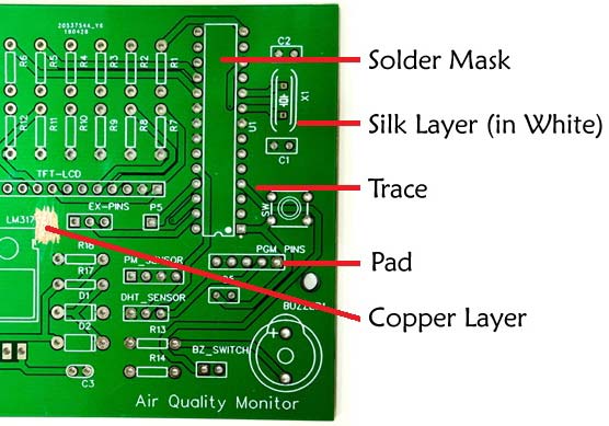
1. Silk Screen Layer
This is the top most layer of the PCB. A Silk screen layer is used to print text, lines, art, logos or any other information on the PCB which will facilitate easy understanding of the board and help in identifying which components goes where. Texts printed on the silk screen are usually white in colour and these descriptions help to make Component placing/assembling, testing, servicing, and sometimes using the circuit board easy. A silk screen servers no engineering values other than merely displaying stuff, it has nothing to do with electronics connection.
2. Solder Mask Layer
This is the green color protective layer that you find on PCBs. The connections between the components on a PCB are made using copper track in the conductive layer, we will learn more about conductive layer in next sub-heading. But now you can think of the Solder mask layer as a layer which comes beneath the silkscreen layer and on top of the conductive layer.
With copper being one of the most common conductivity materials used on PCBs, this additional layer is added on top of the copper traces to prevent the copper from being oxidized from interaction with air. Since this layers masks out the copper traces from being etched during manufacturing process the layer is called solder mask. Asides from oxidation, the solder mask also prevents easy short circuiting of the PCB board which could happen if the copper traces were left bare.
3. Conductivity Layers
Every PCB board comes with a conductivity layers. It is on this layer that all the routes (called traces similar to wires) which connects the electronics components are etched. The conductivity layer could be made of copper or other conducting materials. Depending on the type of PCB, and complexity of the board, PCBs could have single or multiple (up to 12) conducting layers. The connections on a conductive layer is accomplished using Traces, vias and pads.
Traces
We have established the fact that a part of the reason why PCBs are created is to eliminate wires here and there, without the wires, the components still need to be connected one pin to the other, and that is achieved through traces in the PCB board. Traces are etched out routes on the conductivity layer. They are made up of the same material as the conductivity Layer (which is usually copper). In the design of PCBs, traces vary in size (width) depending on the components they need to connect and amount of current that will be passing through the route. This variation is similar to the use of wires with different thickness level to carry different currents.
Vias
Vias are tiny hole like spots common on double or multi-side/layer PCBs. They serve a singular purpose of connecting a trace on one side of the PCB to a trace on another side/layer of the PCB. They help PCB designers get through complex routing in PCB design.
Pad
To allow for easy mounting of components, traces terminate at pieces of copper surrounding holes into which the pins of the components to be mounted. These pieces of copper around the holes in the footprint of components are called Pads (or solder pads). They provide mechanical support for components and are really nothing but a piece of copper to which the pins of components are soldered to connect them to a trace.
4. Substrate Layers
Substrate refers to the solid base on which the conductive layer are laminated. They are usually dielectric composite materials. The composites contain a matrix (usually an epoxy resin) and a reinforcement (usually woven, nonwoven, glass fibers, sometimes even paper), and in some cases a filler is added to the resin (e.g. ceramics; titanate ceramics can be used to increase the dielectric constant).
Type of PCBs
PCBs can be classified into several types based on the following parameters
- Number of Layers
- Material using which it is built
- Physical Outlook
- Package of components to be used on it
Types of PCB - Based on Number of Layers
Depending on the complexity of the circuit/schematics being implemented and other design constraints, printed circuit boards can be designed to have one or more conductivity layers or sides. Based on layers, PCBs can be divided into three type’s namely Single layer PCBs, Double Layers PCBs and Multi Layer PCBs.
1. Single Layer PCBs
Single layer PCB refers to PCBs in which the conducting material (Usually copper) is only spread on one side of the board. The single layer PCBs are the simplest in terms of design as they usually contain fewer components and are the most popular because they are easy to manufacture. As such, they are cheap and could even be home made (definitely not of the same quality as it would be machined).
2. Double-Layered PCB
The complexity of the design of electronic circuits at times makes it difficult to put all the traces to connect components together on a single side. At times even when you can fit the traces, the board becomes too big for the size constraints and with design rules like crosstalk budgets (which we will cover in a later article), the reliability of the boards and overall performance is affected.
In situations like this, PCB Artists/Designers go for double layer PCBs. Unlike the single layer boards, the Double layered board has conducting material on both sides of the board. As such, components can be mounted, and traces etched on both sides of the board to reduce the over population and design complexity. Vias are one of the major enablers in the design of double sided PCBs as they provide a way to connect traces on one side of the PCB to the other.
The two sides of the PCBs are usually referred to as Top and Bottom respectively. An image to illustrate the double sided PCB is shown below.
As much as they help designers reduce complexity in creating traces for single sided boards, double-sided PCBs are usually more expensive, as such, designers should ensure they have explored all design possibilities and have considered how the additional cost affects their product target price before making the jump.
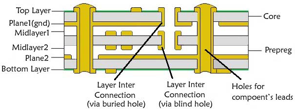
3. Multi-Layer PCBs
These are PCBs with more than two conductivity layers. They are essentially made up of multiple double-sided PCBs glue together with insulation attached. You guessed right, they are used in the design of very complicated electronics, like the “Motherboard” of a PC or something of equal or greater complexity. Multilayer PCBs could have up to 12 layers. Due to the complexity involved in their production, they are usually very expensive to manufacture.
Types of PCBs - Based on Fabrication Materials
PCBs are also sometimes classified based on the kind of materials of which there substrates are made. As earlier said, substrates are usually dielectric materials and the most popular materials used for PCB fabrication include FR4, FR-1 and FR-2, CEM-1, CEM-3, Polyamide and Prepreg
1. FR4
FR4 is the most popular PCB Substrate material for glass laminated PCBs on the market today. The FR in the name stands for FIRE RETARDANT. Based on woven glass-epoxy compounds, PCBs based on FR4 are typically strong.
2. FR-1 and FR-2:
FR1s and FR2s are similar materials made from paper and phenol compounds and are typically used in making low cost single-layer PCBs. PCBs made of these materials are usually of lesser quality compared to the FR4 and are commonly found in consumer electronics. FR1s have Poor moisture resistance and Low arc resistance which makes them sometimes undesirable
3. CEM-1
PCBs Based on CEM-1 have performance slightly greater than those based on FR4 but are generally more expensive. The CEM-1 material is made from paper and two layers of woven glass epoxy and phenol compounds and its only used for the development of single layer PCB boards only.
4. CEM-3:
This material is white coloured, glass epoxy compound which is mostly used in double layer PCB. CEM-3 has lower mechanical strength compared to FR4, but it is cheaper than FR4. So, this is a good alternative of FR4.
5. Polyimide
Polyimide are used as substrates in flexible PCBs. They are a high-temperature polymer made from kepton, rogers, dupont. They are expensive, possess good electrical properties and operate over a wide temperature range with high water absorption and high chemical resistance.
6. Prepreg:
Prepreg means pre-impregnated. It is a Fiberglass impregnated with resin. These resins are pre- dried, so that when it is heated, it flows, sticks and completely immersed. Prepreg has adhesive layer which gives strength similar to FR4. There are many versions of this material according to resin content, SR- standard resin, MR- medium resin and HR- high resin. This is chosen according to required thickness, layer structure and impedance. This material is also available in high glass transition temperature and is halogen free.
Types of PCBs - Based on Physical Outlook
PCBs can be categorized based on their outlooks from rigid to flexible depending on the application in which they are to be used. The common PCB outlooks include Rigid PCBs, Flexible PCBs and Flex-Rigid PCBs
1. Rigid PCBs
Rigid PCBs are easily the most popular of PCBs based outlook. They are present in almost all day to day electronic devices and are made out of solid material which cannot be bent around like flexible PCBs. They can be single, double or multi layered, and are easier to design and manufacture compared to other PCB outlooks. Their Lifespan is typically high due to their rigidity and they are used in all sorts of electronic devices.
2. Flexible PCBs
We are in the age of wearable electronics, where electronic devices are not just held but could be worn as an adornment. Often times to ensure small size, there is a need to be able to bend the PCB to maximize space or create special functions or effects. This is where Flexible PCBs come in. Also known as Flex Circuit, this type of PCB uses flexible plastic material like polyamide, PEEK (Polyether ether ketone) or transparent conductive polyester film as substrate to allow give the flexibility that allows the PCB to be bent in all kinds of manners. Like the other kind of outlook, they can also be single, double or multi sided.
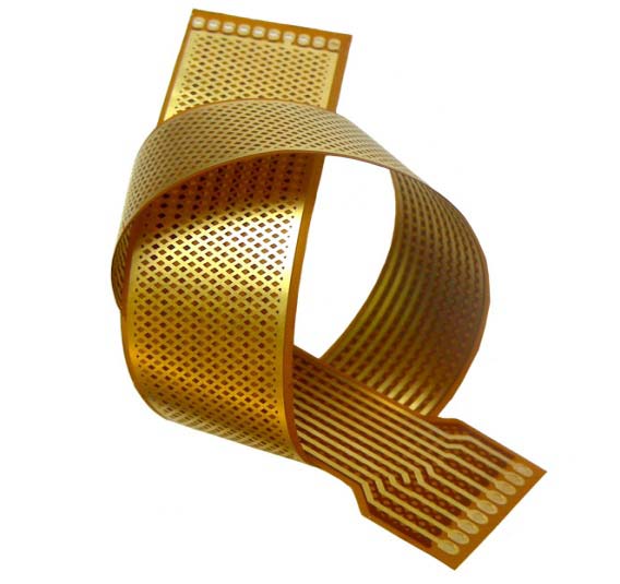
Flex circuits find applications in organic light emitting diode, LCD fabrication, flexible solar cells, automotive industries, cellular telephones, cameras, wearable and complex electronics devices like PCs. Flex circuits are complex to manufacture and also they are very expensive. They are also not as durable as rigid PCBs as the twist and turns tend to take a toll on the PCB especially when it happens regularly.
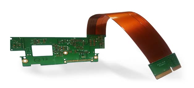
3. Flex-Rigid PCBs
There are situations where several constraints (like size and application) around the design of a device calls for the use of a PCB which is one part flexible, and other part rigid. Flex-rigid PCBs consist of multiple layers of flexible PCB attached to a number of rigid PCB layer. They find applications in devices like cell phones, digital cameras and automobiles etc where multiple boards are stacked on one over the other. An example is shown in the image below.
Types of PCB - Based on Components Packaging/Mounting
Electronic components come either as DIP ( dual in line packages)/with leads or as SMDs (surface mounted). While this probably should just be a type of mounting system for PCBs, it is sometimes used to categorize PCBs into types.
Based on these, PCBs can be categorized into two types namely Through Hole PCB and Surface Mounted PCBs
1. Through Hole PCBs
Through hole PCBs are the type of PCBs designed for DIP based ICs and components with leads. The PCB features drilled holes in which the leads of the components rest and are soldered to the pads which are usually situated on the other side of the PCB. One major benefit in through-hole PCBs is that the holes provide additional mechanical support for the components making their connection to the traces more reliable. However drilling increases the cost of making the PCBs especially in double-layer and multi-layer PCBs where extra care needs to be taking when drilling.
2. Surface Mounted PCBs
For this type of PCBs, surface mounted components are used. These components are usually small in size and are directly mounted on the solder pads without the need for holes. SMD components are usually cheaper and also eliminate the additional cost attached to drilling, as such, the overall cost of a Surface mounted PCB is usually cheaper and the size, smaller compared to through-hole based PCBs.
There are situations where these two mounting approach are combined on a PCB. This probably is a more frequent occurrence than the two earlier mentioned approaches.
Steps to Design a PCB
The PCB design process is synonymous with the process of designing the device itself. There are four major stages involved including;
- BOM Research and Selection
- Schematics Design, Simulation and Tests
- Board Design
- Validation, Verification and CAM Processing
1. BOM Research and Selection
At this stage several decisions are made on the size of the device to be designed, the components to be used and their packages (DIP or SMD), performance, power consumption, cost etc are all figured out at this stage. For best practices, are sort of pre-design is done during the early part of this stage to identify the key parts of the device and evaluate cost among others.
2. Schematics Design, Simulation and Tests
With all the components to be used identified, the circuit is then designed with tests and simulations going on simultaneously to ensure it performs as desired. The Schematics is usually created with the same software to be used for PCB design. More on this will be covered in another article.
3. Board Design
This involves creating the layout of the PCB. Creating the traces, arranging the components, etc. This is usually done using the same software as the one used for creating the schematics. More on this will also be covered in the second part of this series.
4. Validation, Verification and CAM Processing. This is the final stage before sending the board for manufacturing. It involves activities like running a DRC (design rule check) to ensure the design does not contain errors like overlapping traces, too little space between traces, Overlapping solder Pads, Skinny Traces, incorrect mounting holes or drill holes sizes amongst others. Other assessments are also performed to ensure the board is low noise, and meet other requirements. Certain software like KiCAD and others also allows the visualization of the board in 3D, this can be done to get a feel of what the board will look like after manufacturing. With all these done, The Gerber files for the board are then generated. Gerber files are sent to board houses and manufacturers to manufacture the PCB boards.
That’s it for the first part of the series. For the next part, we will look into some popular PCB design software and learn about them. Feel free to reach out to me via the comment section with questions and general comments on any specific part of PCB design process you’d like me to talk about.
Till Next time.

Latest Articles
-

Single-Sided vs. Double-Sided PCBs: Which One Is Right for Your Project?
-

Exploring the Different Types of PCB Layers and its Purpose
-

PCB Connectors: A Comprehensive Guide to the Different Types and Their Applications
-

PCB Soldering Steps
-

Basic Electronic Component Symbols that Every PCB Design Engineer Should Know
-

Home Made PCBs – A Step by Step guide to build PCBs in your Home
Comments