

Exploring the Different Types of PCB Layers and its Purpose
A printed circuit board (PCB) is a thin board made of non-conductive material, such as fiberglass or plastic, with conductive pathways etched into it. These pathways, or traces, are used to connect different components, such as transistors and resistors, on a PCB.
One way to categorize PCBs is by the number of layers they have. Single-layer PCBs, as the name suggests, have only one layer of conductive material, while double-layer PCBs have two, and multi-layer PCBs have three or more layers.
In this article, we will explore the different types of PCB layers and their uses.
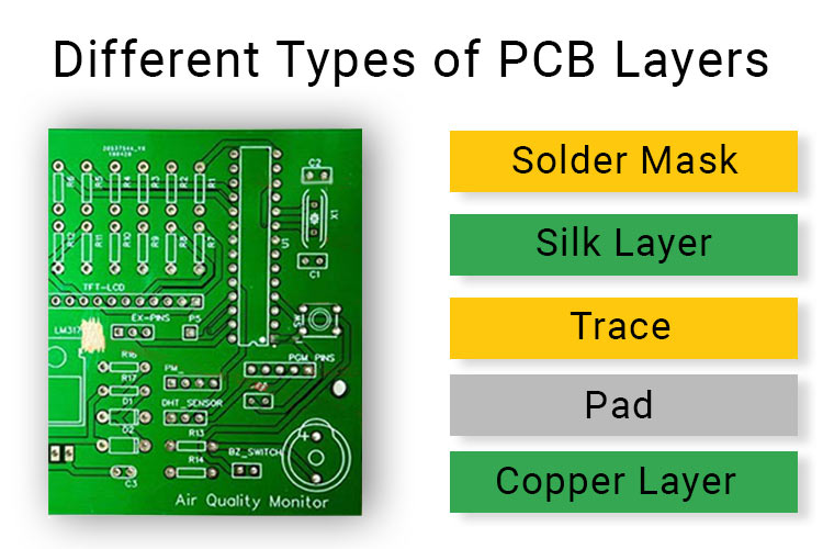
Substrate Layer
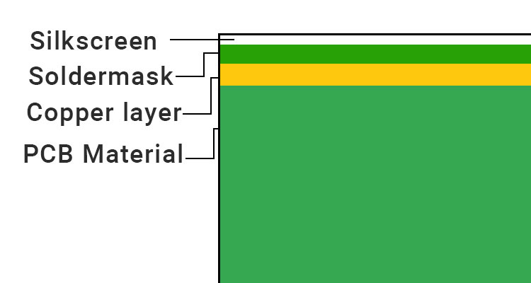
The substrate layer, also known as the base material or core material, is the foundation of a PCB. It is a non-conductive layer made of a material such as fiberglass or plastic that provides structural support for the PCB. The substrate layer is usually coated with a thin layer of copper on both sides, which serves as the conductive layer.
Copper Layer
The copper layer is a thin layer of copper that is applied to the substrate layer on both sides of the PCB. It is the layer where the conductive traces, or pathways, are etched to connect the various components on the PCB. The copper layer is also used to connect through-hole components, such as capacitors and resistors, to the PCB by drilling holes through the substrate layer and filling them with copper.
Solder Mask Layer
The soldermask layer is a thin layer of non-conductive material that covers the copper layer of the PCB. It serves two main purposes: to protect the copper traces from damage and to prevent short circuits. The soldermask layer is usually applied in a specific pattern to expose the copper traces in areas where components will be soldered.
Silkscreen Layer
The silkscreen layer is a thin layer of ink that is applied on top of the soldermask layer. It is used to print labels, such as component values and part numbers, on the PCB. The silkscreen layer is also used to indicate the locations of components and other important information, such as test points and mounting holes.
Types of PCB based on Number of Layers
Single-Layer PCBs
Single-layer PCBs are the most basic type of PCBs and are generally the cheapest to manufacture. As they only have one layer of conductive material, they are limited in the number and complexity of the connections they can make. Single-layer PCBs are most commonly used in simple circuits, such as those found in basic electronic devices like calculators and alarms.
Advantages of Single-Layer PCBs
- Cost: Single-layer PCBs are the most basic and cheapest type of PCBs to manufacture.
- Simplicity: Single-layer PCBs are easy to design and fabricate, as they only have one layer of conductive material.
- Size: Single-layer PCBs are generally smaller and more compact compared to multi-layer PCBs, as they have fewer layers.
Disadvantages of Single-Layer PCBs
- Limited number of connections: Single-layer PCBs are limited in the number and complexity of connections they can make due to their single layer of conductive material.
- Performance: Single-layer PCBs may not perform as well as multi-layer PCBs in high-speed or high-frequency circuits due to the increased risk of noise and crosstalk between traces.
- Component density: Single-layer PCBs are less able to fit a large number of components in a small space compared to multi-layer PCBs.
- Flexibility: Single-layer PCBs are less flexible compared to multi-layer PCBs, as they cannot utilize internal planes for power or ground distribution.
Double-Layer PCBs
Double-layer PCBs have two layers of conductive material, separated by a non-conductive layer. This allows for more complex circuits and a greater number of connections. Double-layer PCBs are often used in more advanced electronic devices, such as computers and smartphones.
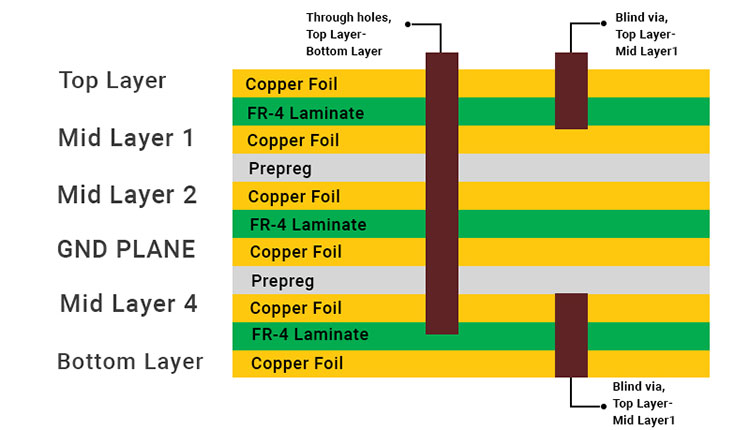
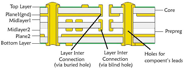
Multi-Layer PCBs
Multi-layer PCBs have three or more layers of conductive material, separated by non-conductive layers. These PCBs are the most complex and are often used in sophisticated electronic devices, such as servers and medical equipment.
Advantages of Multiple PCB Layers
One of the main advantages of multi-layer PCBs is their ability to fit more components and connections into a smaller space. This is because the additional layers allow for more routing options and the use of internal planes, which can be used to distribute power or ground signals.
Multi-layer PCBs also have improved performance compared to single- and double-layer PCBs due to their ability to reduce noise and crosstalk between traces. This is especially important in high-speed or high-frequency circuits.
Conclusion
In summary, PCBs are classified based on the number of layers they have, with single-layer PCBs being the most basic and multi-layer PCBs being the most complex. The number of layers in a PCB determines the number and complexity of connections that can be made, as well as the performance of the circuit. Single- and double-layer PCBs are suitable for simple circuits, while multi-layer PCBs are needed for more complex circuits and devices.

Latest Articles
-

Single-Sided vs. Double-Sided PCBs: Which One Is Right for Your Project?
-

Exploring the Different Types of PCB Layers and its Purpose
-

PCB Connectors: A Comprehensive Guide to the Different Types and Their Applications
-

PCB Soldering Steps
-

Basic Electronic Component Symbols that Every PCB Design Engineer Should Know
-

Home Made PCBs – A Step by Step guide to build PCBs in your Home
Comments