

Home Made PCBs – A Step by Step guide to build PCBs in your Home
Getting a PCB fabricated from a manufacturer requires prior planning and might not be feasible for very low volume. It is also not advisable to approach professional PCB fabricators to build our hobby circuits, that is why in this tutorial, we are going to learn how to build our very own PCB boards at home. Note that this process cannot be used for complex circuits and is not very reliable. But will work for simple low-level circuits like the basic Arduino circuit that we are using in this tutorial and also what is more fun than building your own PCBs. That being said, let's learn how to build your own Arduino boards at home.
Types of Home Made PCBs
There are two popular methods for making PCB at home, one method is the Toner Transfer Method and the other is the Ultraviolet Rays Method. Here, I am going to explain the most popular method which is the Toner transfer method. Both the methods are more or less the same with just one or two-steps that are different. According to me, the Toner Transfer Method is comparatively easier. Also, there are so many ways to run your circuit but making custom PCB is preferred by electronics developer/hobbyist/enthusiast. Besides, it offers great stability, reliability, and most importantly it increases in the life of your self-developed products or projects. If you are developing SMPS (Switch Mode Power Supply) Circuit Board for any other Power Driving electronics circuit PCB, the output ripple factor depends on PCB, and you must use PCB for safety purposes. In cases like that, it is better to opt for professional PCB manufacturers. On the other hand, every electronics guy like me loves to make his self-designed circuit board which also looks beautiful and works like a champ.
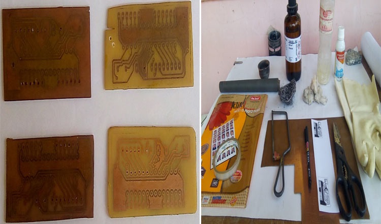
Materials Required to Build your Custom PCB
The following are the materials that are required to build your custom PCB at home.
- The printed layout on A4 Glossy Photo Paper
- Cello tape
- Hacksaw
- Permanent Marker pen
- Scissor
- Coper Coated Board
- Sandpaper
- Steel Wool
- Cotton Wool
- Hand Gloves or Safety Gloves
- Cup
- Muriatic Acid
- Hydrogen Peroxide
- Acid bowl or Acid Chamber
STEP 1: Make your custom PCB Design:
This is the first and very important step. First of all, create your PCB design and circuit diagram using any PCB designing software. If you are new to PCB design, you can check out the following tutorials.
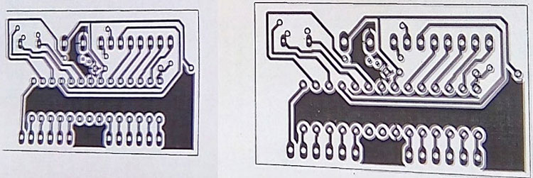
Again, there are many PCB designing software to choose from like, Autocad Eagal, Fritzing, EasyEDA, etc. In my case, I used Autocad Eagle to design the circuit diagram and make a PCB layout both of which are shown below.
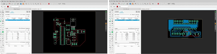
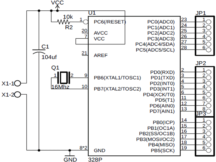
Here are the two screenshots: On the right side is an Arduino project PCB Layout and on the left side is the Arduino board PCB diagram. The complete circuit diagram for a basic Arduino board is shown below
You can also download the PDF of the PCB layout to skip this step and directly proceed with printing the downloaded layout.
STEP 2: Printing your PCB Layout
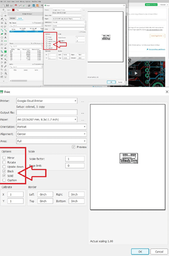
For making PCB, you must print your custom design on a good quality laser printer because we are using Toner Transfer Method to transfer the print on the copper surface using heat, and we are using the copper-coated board as a substrate. Check out the images pinned below.
In a laser printer, there is a dust color (like powder) used to print on the paper using a laser. Also, you have to use thin and glossy photo paper only because it's not possible to transfer the print using normal paper as it absorbs the color instantly. Use only solid black color like no other color works (only black and white combination works for PCB track line) and set 300dpi resolution which is good for this purpose. My printer settings are shown below
STEP 3: Preparing Single Side Copper Board:
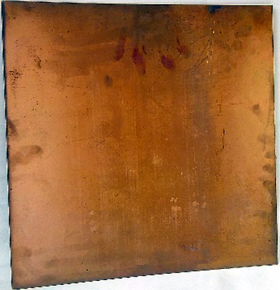
Now, when the designing and printing of all the things are done, we look forward to preparing the copper board first. For this, you have to choose a good quality single side, copper-coated board. You should use the best quality copper board otherwise, the copper layout may be destroyed during the process or even after the entire process is over.
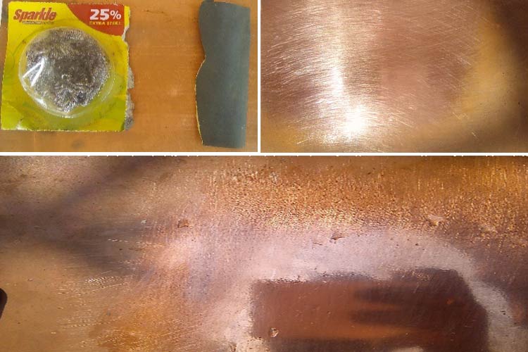
Next, you have to scrub the PCB board copper surface for removing all unwanted dust particles and the copper oxide layer which would have formed with oxygen in the air. I have used steel wool and a small piece of sandpaper and scrubbed the copper surface to make it look shiny, glossy, and beautiful as shown in the picture below. Also, note that you should not use sandpaper heavily, just rub till you get a shiny surface.
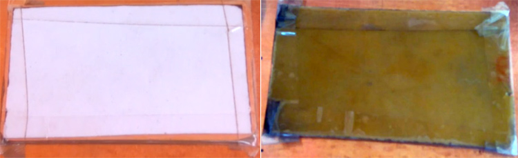
Generally, the coper board comes in full standard size (12 inches in length and 12 inches in width). To mark the area, you need according to your printed layout dimensions using a CD-DVD marker pen and cut the piece using hacksaw cutter.
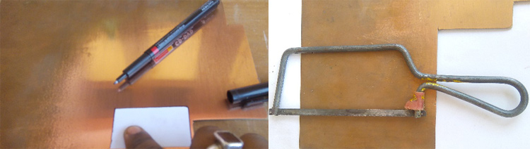
Simply cut out your printed PCB layout design that you printed using a laser printer. Use scissors to cut the layout design on A4 glossy paper and place the printed side on the copper side of the board (make sure there is no dust in between the copper surface and printed layout designed) and fix its surrounded area using tape so that it does not move at the time of ironing.
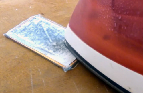
STEP 4: Iron to Transfer the ink to the board
As I mentioned earlier, it is a Toner Transfer Method, so in this step, we will transfer the print from the paper to the copper surface using heat and by putting some pressure at the time of ironing. Do simple ironing over the backside of the paper so that transferring on the copper surface is done easily. Iron for approximately 15 minutes on the set temperature and you will see the paper slightly blackish after 10 to 15 minutes of ironing. It means tonner is successfully transferred to the copper-coated board.
STEP 5: Remove The Paper From The Board
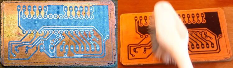
Now, drop it in the hot water and leave it for 10 to 15 minutes to soak the water. After 15 minutes, you will notice paper will get soften. Now, you can rub it gently using your finger and try to peel off layers, one by one. After you have peeled off the first layer, drop it into the water again and peel the second layer. In this way, remove all the layers of the paper and remove the paper completely from the copper board.
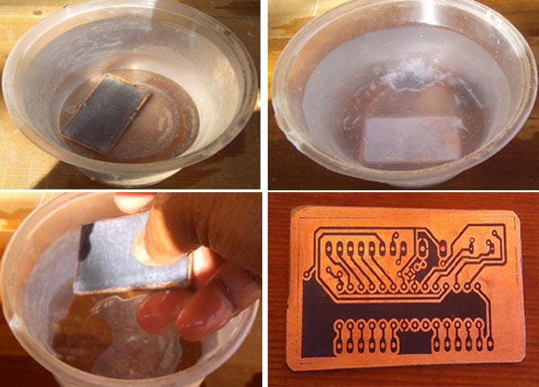
When all the paper layers are removed, you will notice that the PCB surface gets dry, there is still a thin paper layer sticking on the PCB track lines (as you can see in the picture below). It is not possible to remove this thin layer from the copper surface using your finger. To remove this layer, take a toothbrush and drop it into the water. Thereafter, scrub your PCB board track lines and over the layout, and you will notice that the thin layer of the paper layer gets removed.
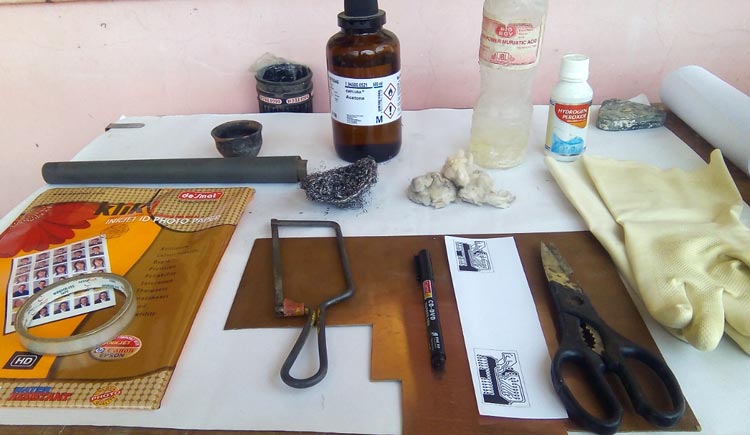
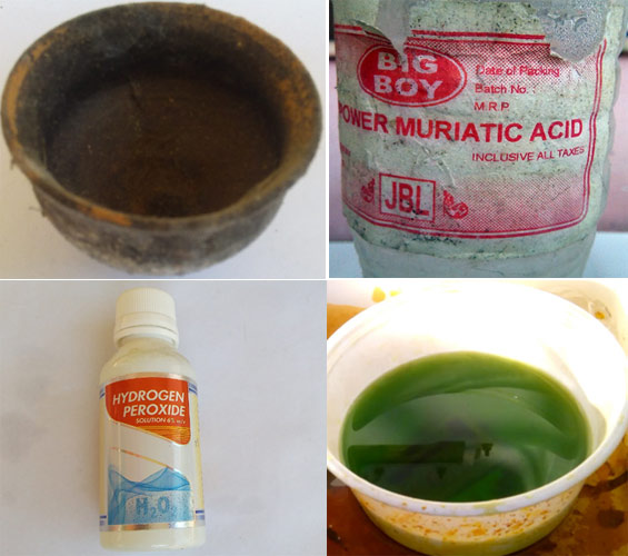
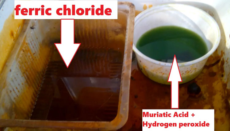
STEP 6: Preparing Acid Solution for Etching the Copper Board:
Now, it’s time to make an acidic solution (wear safety gloves before you carry out this step) for etching the printed copper-coated board. For making the acid solution, normally FeCl3 (ferric chloride) is used. But, here I’m using another method for PCB etching because ferric chloride is not easily available in the area where I live and also it's costly too. Also, sometimes if u want to purchase ferric chloride from a registered chemical laboratory store, they ask for lots of documents and the procedure is tiring. Therefore, I found another very low-cost solution (easily available at your nearest shops) for PCB Etching. Take 3 cups of muriatic acid and 1 cup of hydrogen peroxide mixed in the ratio of 3: 1 in a plastic bowl and make a greenish colored mixture.
The printed area and the track lines on the PCB should be covered with a black color coating (toner) and the outside of the printing area of copper should be removed in this step. So, before dropping it into the acid solution, please check that all the layout and track lines are correctly printed or not. If not, you can use your CD/DVD permanent marker to rectify that track lines on the PCB board. Check out the image given below to see my acid chambers.
STEP 7: Etching your PCB
Now, the acid mixture is ready and you can drop the PCB into this acidic solution and leave it for 15 minutes (Before doing this step, wear safety gloves). For best etching, stir the acid solution repeatedly and periodically after 2 or 3 minutes interval. After completely etching and remove the unwanted copper portions is done, rinse the PCB with normal water.
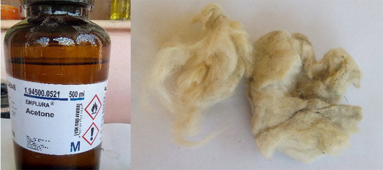
After the PCB gets dry, here is the final step of making the PCB at home. Take a small piece of cotton and take some drops of acetone. Use thinner or nail polish remover to remove this black color (toner) coating from your PCB.
After these processes, your PCB should look something like this shown in the image below.
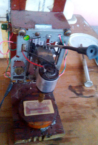
STEP 8: Drill holes for component mounting
Now, you can make holes and insert the component. You can make holes using hand drilling tools or make a homemade drill press machine as I built or else you can purchase the PCB drilling machine too for the purpose.

Latest Articles
-

Single-Sided vs. Double-Sided PCBs: Which One Is Right for Your Project?
-

Exploring the Different Types of PCB Layers and its Purpose
-

PCB Connectors: A Comprehensive Guide to the Different Types and Their Applications
-

PCB Soldering Steps
-

Basic Electronic Component Symbols that Every PCB Design Engineer Should Know
-

Home Made PCBs – A Step by Step guide to build PCBs in your Home
Comments