

KiCad Tutorial 3/5 – Creating Custom Parts and Schematics
In our previous two articles, we explained how to install and start with Kicad and how to create schematics on KiCad and also designed our 7-Segment LED Driver circuit in the processes. For this article, we will look at some of the things we skipped in that article, like creating custom parts, connecting components neatly using the bus tool, Assigning Footprints to symbols and Generating Netlists in kicad, amongst others. We will be continuing with the same schematics we created in the last article to show how these things work. Let's dive in.
Creating a Custom Part Symbols in KiCad
One common task, designers deal with when designing schematics is the need to create a new symbol. New products/components are released every day and it’s possible that the symbol for the particular components you want to use is not yet available on KiCad and a library containing it is not available online, this usually put designers in a situation where they have to create their symbols for components. While this is a tedious task in most EDA software, it is simpler in KiCad because the symbols for a component are separated from its footprint, as such, similar footprints can be assigned to similar components, reducing the amount of work the designer would have to do.
There are about 4 different ways through which new schematic symbols can be created in KiCad.
- Using Component Library Editor
- Modifying Existing libraries
- Making Schematic symbols using quicklib
- Making Schematic Symbols with Python Scripts
To keep things simple, for today’s article, we will be focusing only on the first method that is creating schematics using the Component Library editor. To demonstrate how this works, we will be creating a sample symbol for an imaginary component. Since this new symbol has to be stored in a library we will also be creating a new KiCad library.
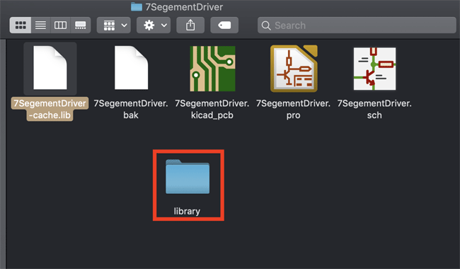
Start by going to the same folder as our last project and create a folder called library within it. Our library, when created, will be stored in this folder.
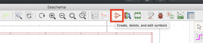
Next, launch the KiCad EEschema, click on the symbols edit icon, located on the top toolbar (highlighted below).
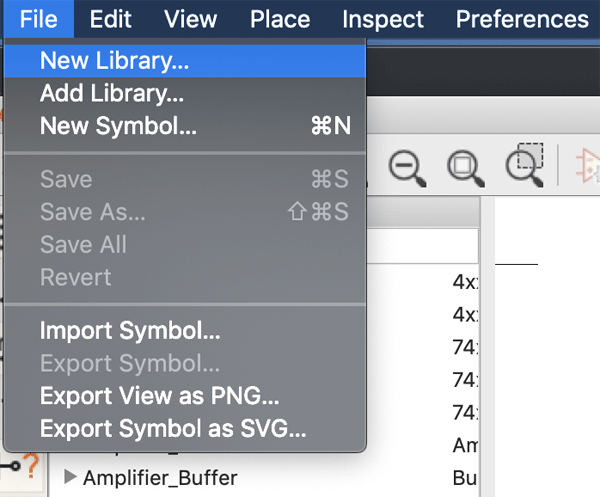
It will launch the Kicad Symbol editor dialogue box. As soon as the dialog box (shown below) opens, click on “File” on the title bar and select the new library.
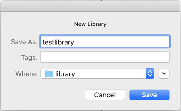
This will create a small dialog box, which will allow you to enter the name and location of the library you wish to create. Set the location to that of the folder we created initially. I will be calling the library test library, but feel free to call it whatever you want.
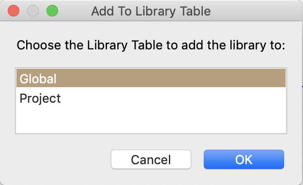
Clicking on the save button will launch a small dialog box that will ask if you want to create the library specifically for that particular project or for global usage. Select global usage so the library is available for all your KiCad projects.
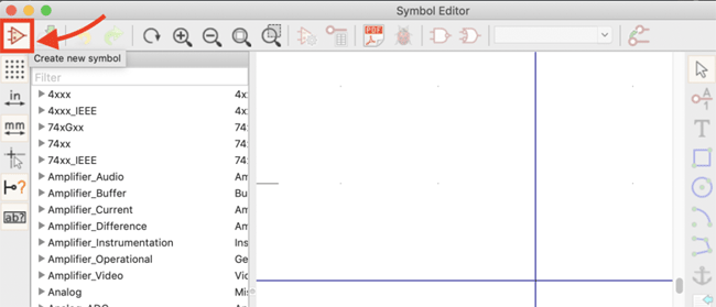
With this done, we can now add symbols to the library. Click on create a new symbol button indicated with the arrow below.
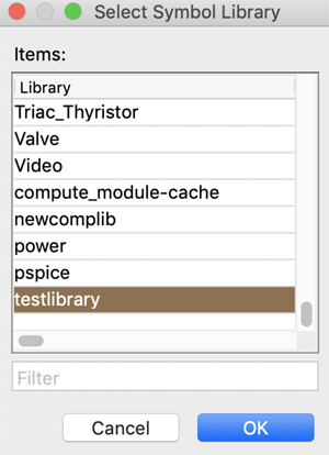
This should launch a dialog box that will ask you to select a library to which the symbol will be added. Scroll down to the library we just created and click ok.
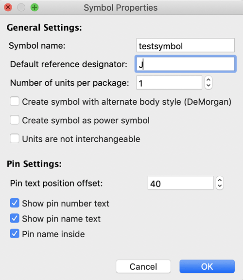
Next, another dialogue box will pop up asking you to fill in the properties of the symbol; its name, reference, number of units per package and other options. Set as shown in the image below.
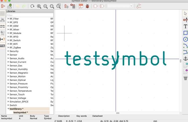
Click on the Ok button. The Symbol editor should now look like the image below with the name of your symbol written on the canvas.
Adding and Labelling pins for Custom Symbols
Next, we need to add some pins to the symbol. This is done using the add pins icon ( ) (2nd icon below the cursor symbol) on the right toolbar. To place a pin, left click in the center of the part editor sheet just below the name label. This will open a dialogue box (shown in the image below) for you to fill in the details of the pin.
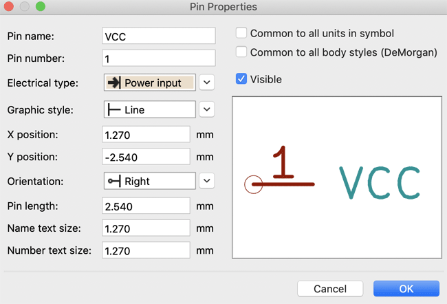
One of the key properties of pins is their electrical types. Pins could be input, output, passive, power in, power out, etc., For power pins like VCC which brings power in, you can select electrical types like power input, while for signal pins which could be input or output, you can select passive.
Pins could also be hidden or visible. Hidden pins are pins to which you probably do not need to connect to during the schematics. You can look up the other properties to get what each one stands for. To show how this works, we will assume the component whose symbol we are trying to create has 3 pins; VCC, GND, and signal.
Create the first pin, VCC by filling out the pin properties dialog box as shown below.
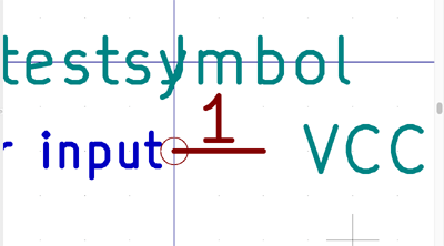
Click on the OK button and then position the Pin where you want, just below the label.
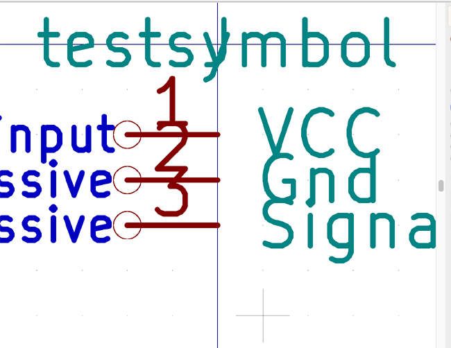
Do this for the remaining pins setting the electrical type as passive for both the ground pin and the signal pin, such that the canvass looks like the image below. Feel free to rearrange the components as you want using the same hotkeys used in EEschema (move - m, rotate - r, etc.) that we discussed in our Introduction to KiCad Tutorial previously.
Creating an Outline for Custom Symbol
Next, we create a shape/outline for the component. This can be done using any of the drawing icons on the right toolbox including; rectangle, line, ellipse. For this, we will create a simple rectangle box as an outline for the symbol. Click on the rectangle tool, click on a starting point on the canvass and an endpoint. This should draw the box such that your canvass now looks like the image below. Move your mouse over the symbol name and use the move hotkey (m) to separate the reference from the symbol name such that “j” is now placed below the component.
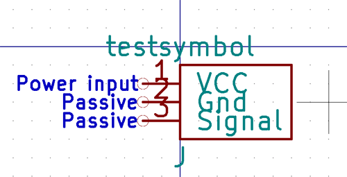
With this done, your library is now ready. Click on the save all changes icon to save the symbol and update the library.

Saving and re-using Custom Symbol on KiCad
The symbol should now be saved and be available for use in all of your KiCad projects.
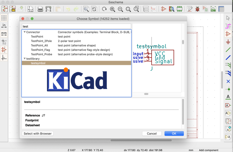
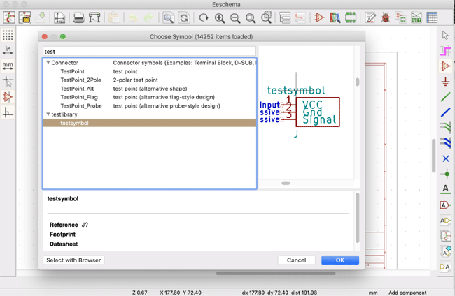
To test things out after saving, close the symbol editor, go to EEschema and press “a” on your keyboard to add a component to the canvass. Search for the new component we just created. It should pop up like in the image below.
Let’s stop here for now. If I get time I will also write on how other methods of creating component symbols work in a later tutorial. If you have any particular requirements leave that in the comment section and we will discuss that.
Adding New Component Library
There will be situations where the symbol you need has already been created by someone else and exist in a library that is not among the default KiCad libraries. To be able to use that symbol, you will need to either import the library into the symbol library for your current project, so it's available to the project alone, or import it into the general global kicad symbols library. You can follow the steps below to know how to add a library downloaded from the internet.
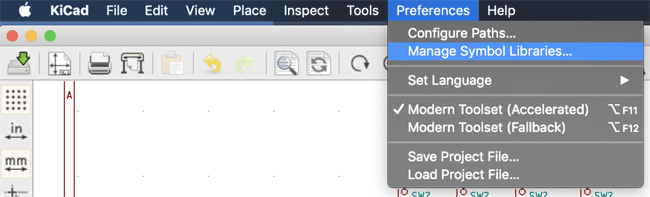
1. On the EEschema page, click on preferences on the title bar and select manage symbol libraries from the drop-down.
2. On the window that opens, you will see two tabs; global libraries and project-specific libraries. This is where you choose whether it's going to be a library specifically for a project or it will be available (“globally”) for use by other kicad projects.
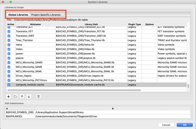
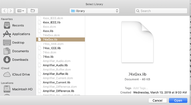
3. The first step to install a library will be downloading it from the internet or copying from somewhere. To install a library in KiCad, click on the folder icon on the page above and navigate to where the library is. As an example, we will be using one of the pre-installed libraries. So navigate to the kicad library folder. Its location depends on your Operating system but the path is always indicated under the “path substitutions”. Select any of the libraries and click open.
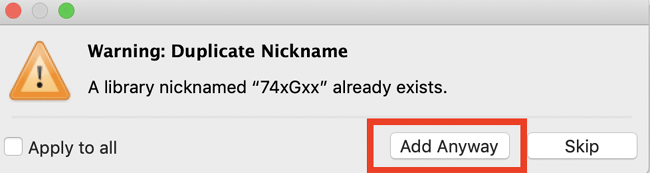
4. Because the library already exists, it will ask for confirmation about adding it. Click the Add Anyway option.
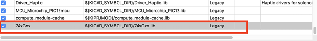
5. The library should now be available at the end of the list. You can delete it to prevent any confusion for this project or just rename it and click ok on the symbol libraries page.
The components/symbols in that library will now be available for use in your project. This method can be used to add multiple libraries, delete libraries, etc.
Connecting Components Using Buses and Labels on KiCad
In the last article, I mentioned there are several ways through which components can be connected one to the other and we explored connections using the wire tool. The other wiring tools which can be used to wire components on KiCad are Nets and Buses. We will pick them one after the other and examine how to connect components neatly and effectively using these means.
1. Connecting Components using Nets
To demonstrate how this works, we will be using the same schematics we created in the previous article. Locate it and open it on EEschema. With that done, select the “place netlabel” icon on the right toolbar to pick the net labeling tool or press the hotkey “i”.
With the tool selected, click on wires that are to be connected and label them with the same name. This will create an invisible connection between them, making the schematics neat, easy to read and pleasing to the eye which is very useful when creating complex schematics.
Let’s try this on the wire connecting resistor “R1” and a pushbutton “A1” to pin “DA” on CD4511.
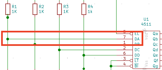
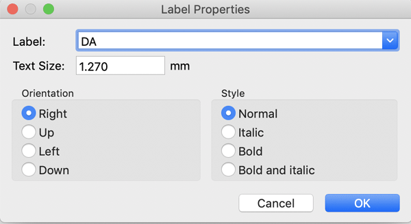
Delete this wire by right-clicking and selecting delete or by using the “delete” hotkey. With the wire deleted, click on the tip of the pin “DA” with the “place netlabel” tool selected. This will launch a dialog box that will allow you to name the label, and enter other properties of the text (name). Let us label this wire “DA” after the pin. Fill the dialog box, such that it looks like the image below and click Ok.
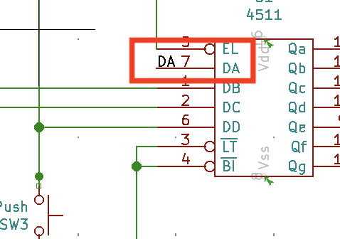
You should now see the label name attached to the mouse/cursor. Move it around and place it at the tip of the pin DA, such that the pin becomes labeled as shown below.
Next, click on the wire connecting pushbutton A1 to Resistor R1 and name that “DA” also, Same as the first one.
With this done, the wire joining R1 and pushbutton A1 to pin DA becomes automatically connected, invisibly. Running a DRC check will help us check for any error in our schematics as a result of this change. You can check the previous tutorial to learn how to run a design rule check.
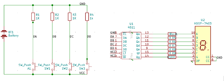
To ensure you understand the process you can repeat it for a few more components such that the canvass looks like the image below.
2. Bus connection
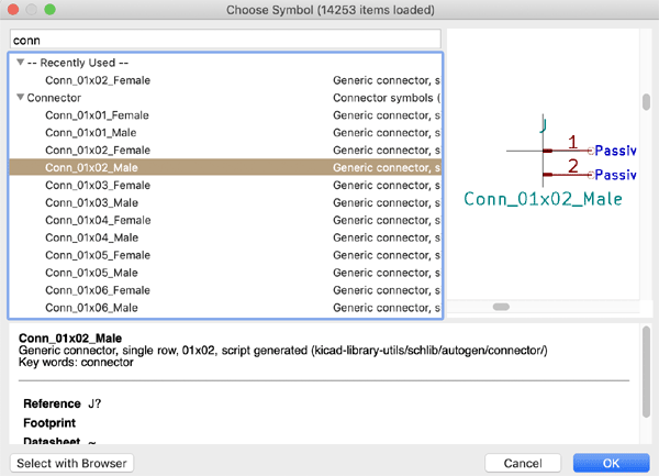
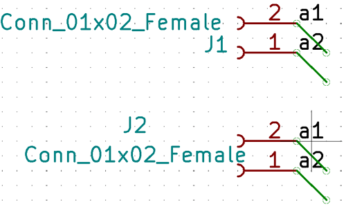
Another method of connecting components of sequential pins is via the use of the Bus Connection. Bus connections are usually used in scenarios where you have, say an I2C or SPI connection where you need to connect sequential multiple pins on one part to pins on another part. To check this feature, we will be connecting three 2-pin connectors together. Search for the connectors as shown below.
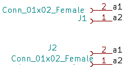
Duplicate the connectors using the “c” copy hotkey so you now have three of them on the canvass. Using the netlabel tool we will label the first pin of J1, as a1. After labeling, we will use the hotkey “ins” to repeat the last action performed, to label the second pin. Press insert, you should see the second pin of J1 automatically labeled (a2) such that it looks like the image below. This working properly depends on you labeling the first pin properly.
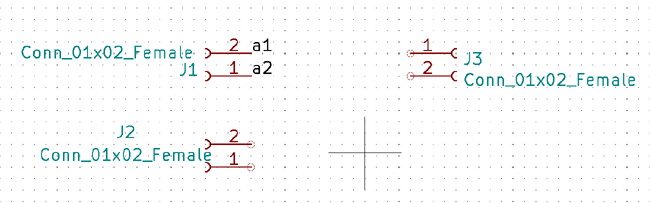
Do the same for J2.
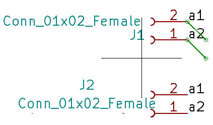
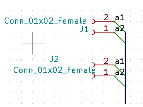
With this done, the two components are automatically connected pin to pin. For the aesthetic purpose and easy evaluation of the schematics, bus nets are then used to show the connections. To do this, select the “place wire to bus entry” tool and click on pin a1 of connector j1. You can also use the “insert” hotkey to repeat this action for the second pin.
Repeat this step for connector J2, such that the canvass looks like the image below.
Then join them together using the place bus tool.
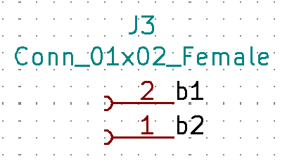
That’s all. Now let’s assume for some reason, there exists another component we wish to connect to the bus, but the netlabel on its pin is different, we can still connect it using the netlabel and the bus tool. Label the pins on connector J3 as; b1 and b2, just like we did for the previous connectors.
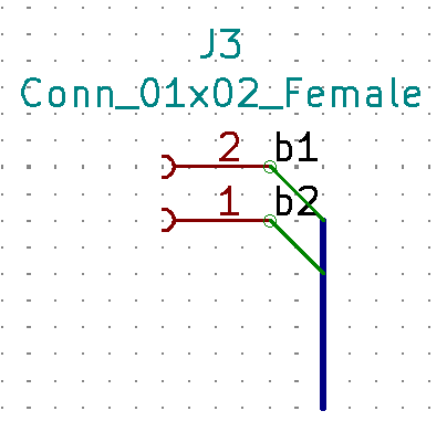
Then select the “place wire to bus entry” tool and click on pin b1 of connector j3 and use the repeat item hotkey to generate the same bus entry line on pin b2. Connect them together using the place bus tool. Such that it all looks like the image below.
Then, Label the bus to which b1 and b2 are connected as “jb1..2” or whatever other name comes to mind. Label the bus to which connectors j1 and j2 are connected as “Ja1..2” or any other similar name.
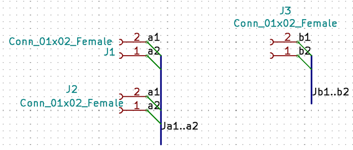
Now use a bus line to connect “jb1..b2” to “ja1..a2”.
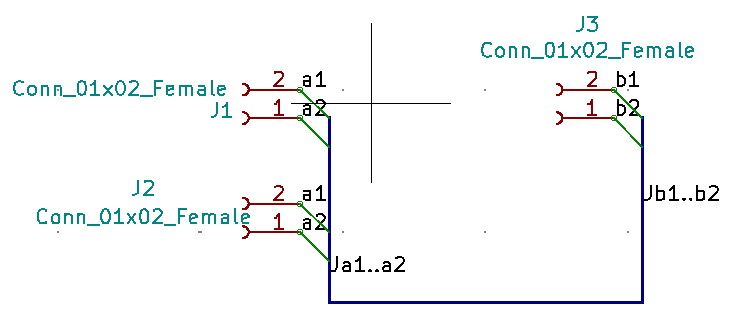
By connecting the two buses together, pin a1 will now be connected to pin b1 and pin a2 to pin b2 on the PCB. This can be done for any number of pins and it’s one of the great ways to move quickly and neatly when creating a large project.
Preparing for PCB
After creating the schematics, there are two tasks commonly performed to get ready for PCB design and manufacturing. They are;
- Generating the netlist and assigning footprints
- Generating the Bill of Materials
To wrap up the schematics section of this tutorial series on Kicad, we will discuss each of the above.
1. Generating the Netlist and Assigning Component footprints to Symbols
As mentioned during the introduction, Kicad requires users to assign footprints to components independently. This may be tedious to a first time Kicad user, who has worked with other EDA software where footprints are automatically assigned, but the user will start appreciating the immense flexibility this gives, as they get more familiar with the tool.
Once the schematic is complete and DRC checks performed, the next task is usually creating the netlist. It is to the netlist that we will add the footprints of the components which will be used for developing the PCB.
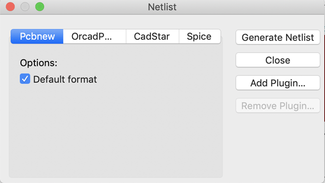
To demonstrate this, we will be using the same schematics we created in the last article. Click on the “generate netlist” icon  . This will launch a window that will ask what software the netlist should be generated for. Select PCBnew, and click on the Generate Netlist button.
It will bring up a dialog box for you to create a name for the file. Use the same name as the project and save it in the same project folder.
With this done, we can now proceed with assigning footprints to symbols. To do this, we will be using the “Assign footprints to PCB” tool  . Click on its icon right beside the “Generate netlist” icon to start.
On clicking the icon, it will launch a dialog box that will allow you to link all the components you used in your schematics to a footprint. The window comprises of a pane at the center which shows all the components used in your schematics, panel at the sides shows the symbol libraries(left panel) and suggested/filtered symbols(right panel).
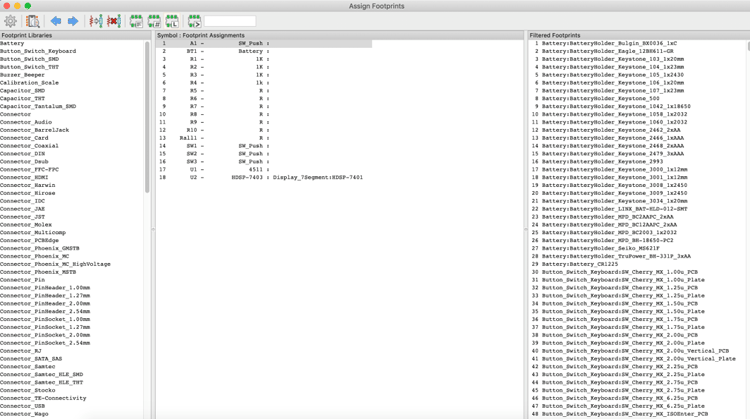
Click on any of the components, then check the filtered footprints to see if there are any of the suggestions that match your desired footprint. If there is, select them by double-clicking on the desired footprint. You can search through the footprint libraries on the left pane, or use all the tools on the top toolbar which includes a tool to view the 3d image (highlighted red) of the footprint and other tool(s) to help you filter your search (highlighted blue). Play around with the tools and assign your footprints like below.
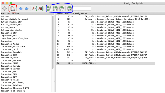
I have left the last two components out to give you a bit of an exercise and help you understand how it all works better.
Go to File and select “save schematics” or use the “apply, save and continue” button, when done to save all changes. You can then close the footprint window and go back to EEschema where we now need to update the netlist by regenerating it. Click on the netlist icon again to update it.
With this done, everything about the schematics is ready.
It is important to note that, at this stage, you must consider every element of your project, from size to cost and outlook, as these factors may contribute to the type of components you choose to work with either SMDs(surface mounted) or THTs(through-hole types).
Of course, there are scenarios where the symbols you need do not exist in kicad. I will be demonstrating how to create your own symbol during the article on creating the PCB.
2. Generating BOM
Lastly, BOMs are an important part of electronics product design. You need to ensure the parts you have selected, are available and affordable amongst others. Aside from these, there are scenarios where firms could also want to place orders for parts early to avoid logistics-related delays. For large projects, it could be tedious to write out the components one after the other. With kicad however, designers could generate a CSV containing all the required components with the click of a few buttons.
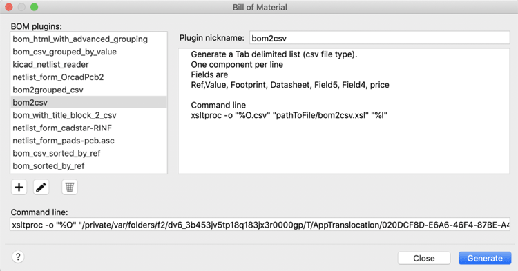
To generate the BOM, on EEschema, click on the “Generate BOM” icon. This will launch a window where you will be asked to select a BOM generation plugin. Select any of the existing ones or add a plugin if none exists. I prefer the BOM2CSV plugin so we will select that and click the generate button.
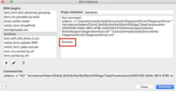
If successful, you should see success displayed on the window.
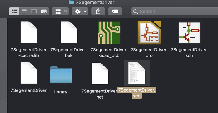
The CSV file should now be stored in the same folder as the rest of the project files.
With this done, we are now ready to move to create the PCB for the project in the next tutorial.
This will be the focus of the next post. Do reach out to me via the comment section if you have any questions or suggestions.
Till next time.

Latest Articles
-

Single-Sided vs. Double-Sided PCBs: Which One Is Right for Your Project?
-

Exploring the Different Types of PCB Layers and its Purpose
-

PCB Connectors: A Comprehensive Guide to the Different Types and Their Applications
-

PCB Soldering Steps
-

Basic Electronic Component Symbols that Every PCB Design Engineer Should Know
-

Home Made PCBs – A Step by Step guide to build PCBs in your Home
Comments