

KiCad Tutorial 2/5 – Drawing Schematics on KiCad
We have already discussed how to select PCB designing software and compared the KiCad with other software. We also covered installing KiCad and its file structures in the first KiCad tutorial. To take things further, we will examine how to develop the schematic diagram for your printed circuit board using KiCad. We will start by creating a KiCad project and work with the EEschema interface, along with placing components and connecting them according to your circuit design.
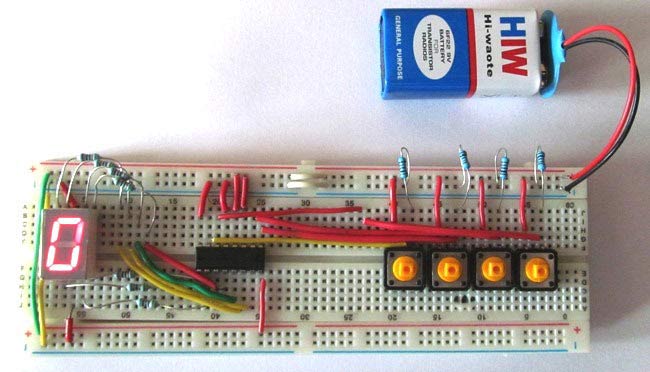
In this process of learning, we will also build an example project, which will be creating a 7-segment display driver circuit using the CD4511 BCD to 7-segment driver IC.
Setting up a New Project
Following our workflow flow chart described in the last tutorial, the first step is creating a PCB, is creating the schematics. In Kicad, this can be done by either creating a new project or launching EEschema directly. However, creating a new Kicad project is usually the more advisable route as it helps keep all the files related to the project in one place, connected to one another. This makes things like correcting the schematics and having them reflect on the PCB easily.
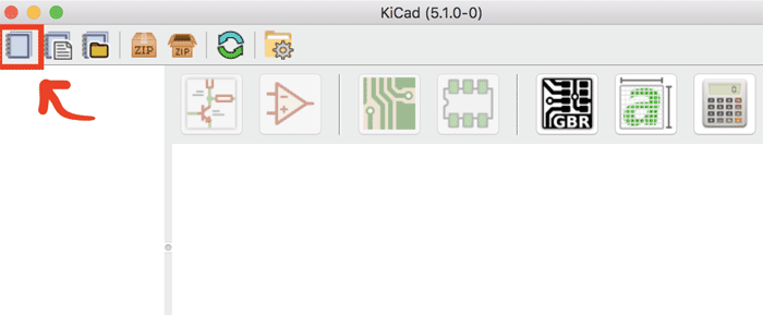
To start, Launch KiCad. The window which opens should be similar to the one in the image below. Click on the new project icon or click on File > New > Project
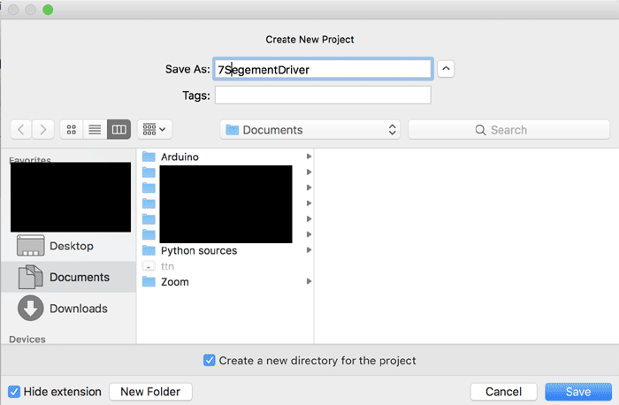
It should open the Create New Project dialog box where you can enter the project name and any other desired information. Enter the necessary details and hit save. We are going to call the project 7segementDriver. Feel free to call it anything else.
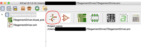
With this done, your KiCad Screen should now look like the image below with the schematics and PCB Layout files created.
Launching EESchema
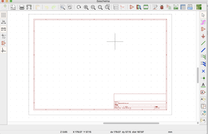
Double click on the Schematics file (with .sch extension) in the Kicad project window or click the schematics icon  (highlighted in red above) to launch EEschema. It should open as shown in the image below. The areas enclosed inside the red double-column are called a schematic sheet and the white area inside it where we will draw our schematic is called a canvas.
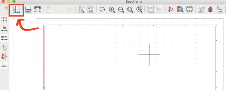
The EEschema, as described in the last article, allows you to create electronics schematics that could then be transferred to create the PCB for your project. With the page open, start by editing the page information including the information for the project title block. To do this, click on the page setting Icon.
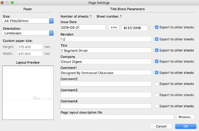
This will create a dialogue box for you to enter the information about the project, from page settings to project name, project version, and information about the company. Fill in the name of the project and the rest as you desire. Then click the save button. Assuming we were creating child sheets, you can check the “export to other sheets” checkbox so the information you fill is applied to other sheets automatically.
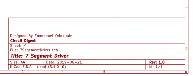
With this done, you should see the changes reflect on the title block as shown below.
Creating the schematics
We can now proceed to start placing components on the canvas to draw our schematics. Creating schematics involves picking components from the Kicad library and connecting them as required. It is usually advisable to draw the schematics down on paper before implementing on EEschema to make things easier.
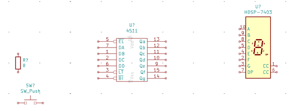
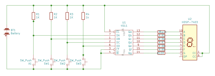
As mentioned in the introduction, for today’s article, we will be creating a schematic for a project which involves driving a 7-segment display using the CD4511 IC. The CD4511 IC is a BCD to 7-Segment decoder/driver IC, which is capable of converting a binary number into a decimal number to be displayed on the 7-segment. For example, to display the number “2” on the 7-segment display we will need to apply digital signals representing 0,0,1,0 (0010) to the A, B, C, D inputs of the CD4511 respectively. These input signals are achieved by the use of Push Buttons which will also be included in the design. The major benefit of using the CD4511 driver IC is its ability to reduce the complexity and number of pins required to connect and control the 7-segment display.
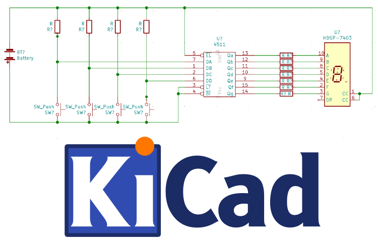
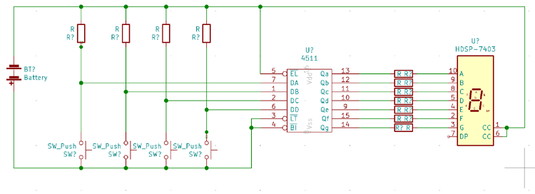
As mentioned above to make things easier, it is usually better practice to have a clear idea of the circuit to be created or at least the bill of materials before proceeding to implement the schematics in software. From the tutorial mentioned above, our schematics are expected to look like this.
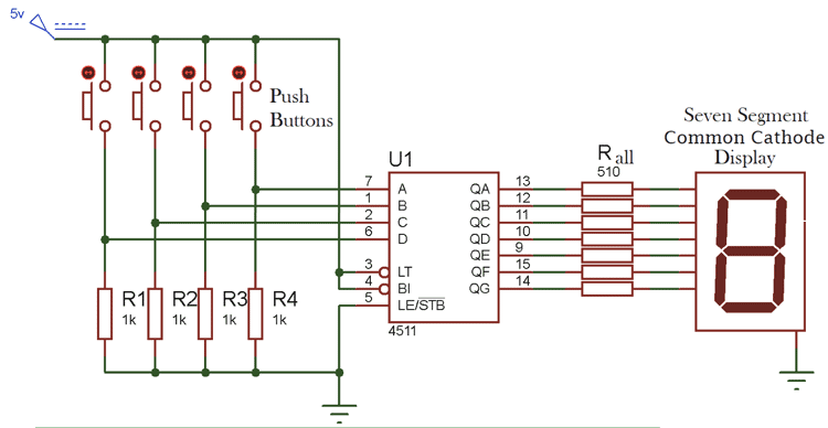
To give a brief explanation of the circuit before we begin, we will provide digital input through push buttons, to Pins 1, 2, 6, and 7 of the CD4511 to provide Binary Coded decimal input. Pin 5 of the CD4511 is connected to ground as we are using the pin to strobe the output and the remaining Pins 9, 10, 11, 12, 13, 14, and 15 are connected via resistors to the 7-segment display.
Placing the Components
To jump to it, we start by adding all the components that are required for the project on the canvass.
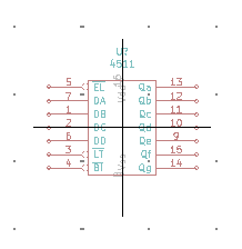
Components in EEschema are referred to as symbols. To add components to KiCad schematics, click on the add symbols icon  or press the hotkey “a”. This will open up the symbols dialog box shown below. Use the filter bar at the top to search for the name of the component and select the right one.
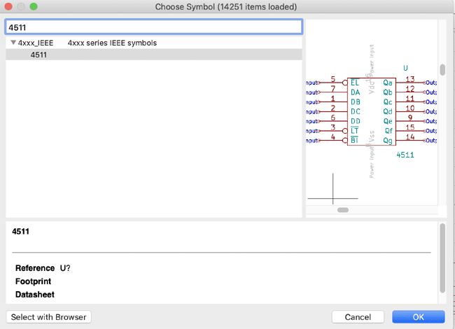
With the component selected, click on the “ok” button. The component should now be attached to your mouse. Drag it to where you’d like to place the component on the canvass and click at any required point to place it.
Following this same process, place the remaining components, including;
- 7 segment Display (Common Cathode) (you can use the HDSP-7403)
- Pushbuttons (4)
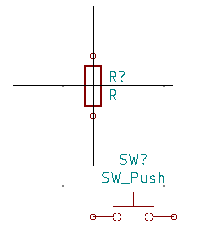
- 1k(4) and 550(7) ohms resistors
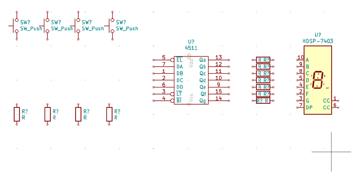
Such that the canvass now looks like the image below with just four components.
We need to add more than one resistor and button for our project. To make things fast, we will be using the duplicate hotkey to create a required number of similar components, that is 11(both values combined) resistors and 4 pushbuttons.
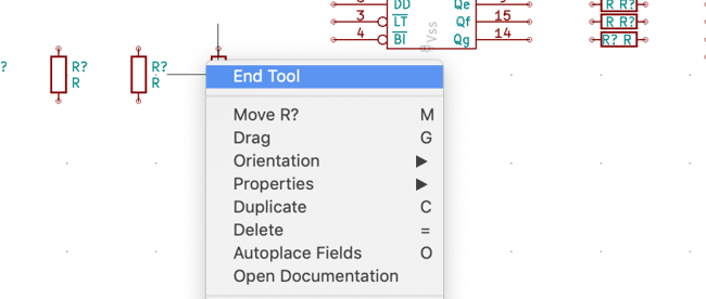
To duplicate, place the cursor on the component/symbol as shown in the image below and press “c” to copy a component symbol. This will copy the symbol and attach it to your mouse cursor such that it can be placed anywhere by clicking at any required point.
Do this to create all the remaining resistors and push buttons along with the power source (battery). Arrange the components such that the canvas now looks like the image below, using the move hotkey - “m” and the rotate hotkey - “r” which also works when the cursor is placed on the component like before.
To move or rotate a block/group of components, click down and drag the cursor over all the components to be moved or rotated then press the hotkey. Highlighted components will be movable by default so you may not need to press the hotkey for that. You can also right-click on a component or a group/block of components to perform several other actions.
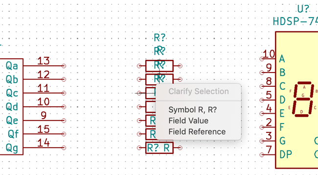
When the hotkeys are pressed at a point where you have multiple components overlapping, it will provide you with options to indicate which of them is to be affected by the actions of the hotkey.
There are several other actions associated with placing symbols on the canvass like; creation of new symbols, import of symbol libraries into kicad, etc., but they will all be covered in the next tutorial to prevent information overload.
Connecting the Components/Symbols
With all the components placed and arranged neatly, it is time to wire the components to one another as you will do with jumper wires on the breadboard. While there are several ways to connect components on Kicad, for this part of the tutorial, we will only be covering connections via the wire tool. More ways to connect the symbols, like the use of the netlabel tool and bus tool, will be covered in the next tutorial.
To connect the components, Select the wire tool  from the right-hand side of the EEschema window and click on the pin of the first component then drag the wire and click on the pin to which it is supposed to be connected.
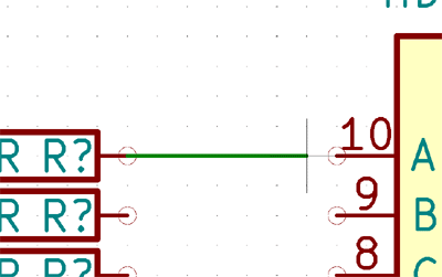
Do this, connecting one pin to the other until the schematics look like the image below.
Add values and annotation to Components
With this done, we can now decide to add the values/ratings/specifications of each component or rename them. Do note that these could be done at any other time during the design and doing it at this point is just a personal preference.
To edit the value labels of each component, all you need do is move the mouse cursor over the component and press “e” to edit component values on your keyboard (hotkey) or right-click and select edit properties.
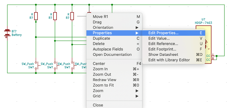
This will launch a dialog box where you can edit the values, name, etc., associated with that particular symbol.
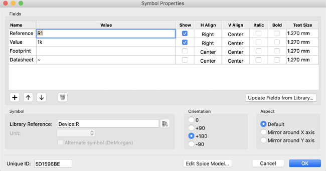
Do these for all the components you deem fit.
Another way to edit the label (not values) of components/symbols is to use the annotate button  on the top toolbar. Clicking on it opens the annotate dialog box and allows you to choose several options including annotating the whole schematics or a specific part, retain the previously annotated symbols or start afresh among other options. We will select the entire schematics option and choose to reset the previously annotated symbols.
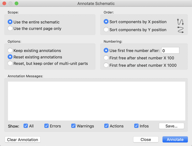
Click on the annotate button and confirm it. With the annotation complete, you should now see it reflect on the components as the question marks in the labels will be replaced with numbers.
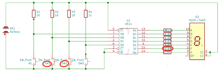
A detailed and clear Annotation is important for BOM as it helps you trace, which components go where.
Schematic Design Rule check on KiCad
To conclude the schematics creation process, we perform an electrical rules check on the schematics which can be done via the design rule checker tool  . Click on it and click run on the dialog box that opens. It will show which pins are not properly connected and other possible errors.
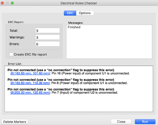
As shown above, it found some errors with our schematics, a small green arrow will appear on the schematic in the position where the error or warning is located. However, since these are pointing to pins we deliberately did not connect to, you can close it and ignore it.
That’s it. Our Schematics is ready and should look like the image below.
To prevent information overload, we will stop here for this article and continue in the next one with how to Generate a netlist, select the PCB footprint for your schematics and other tips and tricks related to the efficient and fast development of your schematics before we move into development of PCBs based on the schematics.
Till Next time.

Latest Articles
-

Single-Sided vs. Double-Sided PCBs: Which One Is Right for Your Project?
-

Exploring the Different Types of PCB Layers and its Purpose
-

PCB Connectors: A Comprehensive Guide to the Different Types and Their Applications
-

PCB Soldering Steps
-

Basic Electronic Component Symbols that Every PCB Design Engineer Should Know
-

Home Made PCBs – A Step by Step guide to build PCBs in your Home
Comments