

PCB Design Guidelines for Assembly (DFA)
Assembly in PCBs involves combining the board with other components, such as the connectors, heat sinks, enclosures, etc, to make up the full product. PCB assembly should be put into consideration early enough during the design process so that we do not end up with a PCB that does not fit right into our product.
When you overlook the assembly process during the design process, problems are highly likely to emerge. The board, in isolation, may appear entirely correct, but when it comes to assembling, it may not fit with other components. It may even lead to a non-functioning product or a product that has performance issues.
Therefore, you should consider assembly during the design process to ensure that the board easily fits with other components during the assembly process. For every decision you make during the design process, you should ask yourself how it will affect the assembly process. If the decision makes the assembly process longer or harder, then you should reconsider.
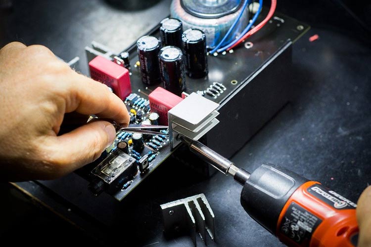
Design for Assembly (DFA) seeks to incorporate some steps into the design process that help and enhance the ability of the assembler to efficiently and correctly attach the components to the fabricated PCB. There are two stages in the assembly process, namely the prototype Assembly and production assembly. You must consider these two stages as part of the DFA during the design process.
Prototype Assembly
This is the process where a prototype is assembled for testing purposes. The prototype tests whether the components should be attached securely and correctly. You should adhere to the clearance and tolerance restrictions. During the design process, you should ensure the following DFA measures are observed
- Components should match their pads.
- The spacing of the components should be adequate.
- Components markings and identifications are accurate and precise.
- Drill-hole rules, such as aspect ratio and hole tolerance, should be applied.
- Correct application of solder mask guidelines
- Thermal relief should be adequate.
- Board edge clearance rules should be applied
Production Assembly
Productions assembly follows the same measures as prototype assembly, and farther takes into account high volume production, component reliability and availability, and testability. During the design process, you should ensure the following DFA measures are adhered to, in addition to the ones in prototype assembly
- The shape should allow for penalization
- Define the types of quality controls that should be used
- The components should be readily available
- The board should withstand the conditions it will be subjected to, such as vibrations.
PCB Design For Assembly (DFM) Guidelines
The following guidelines are helpful during the design process in ensuring the efficient and easy assembly of the board and other components.
Use standard and common components: Should ensure that the components you plan to use are readily available. Also, you should validate their continued production to avoid having components whose end of life (EOL) is approaching as it will minimize delays in the future. Standard and readily available components result in reduced costs, higher quality, and lower inventories. Unique parts lead to increased costs and high chances of poor quality.
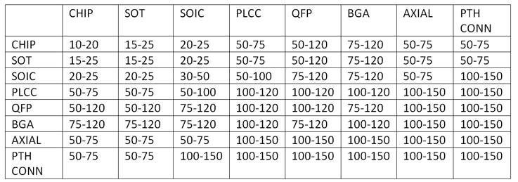
Component Spacing Rules: You should design the board, ensuring that you carefully place the components in a way that they are not too close or too far from each other. No component should overlap with each other. A component placed too close to another cause issues that may require redesigning. To prevent spacing issues, you should ensure that you design your footprint in a way that allows enough gap between the boundaries of each component. The below table shows how much space should be left around each component for different types of IC packages.
Component Orientation and Handling: The board must be designed in a way that components consistently orient themselves when assembled. The orientation of components can cause issues. For instance, issues arise when polarized capacitors and diodes face different directions. The placing of the components determines whether the board can be assembled or not, the soldering techniques which will be used, and the types of thermal reliefs that are required. Also, it affects the quality of signals as some components generate electrical noise when placed too close to others. For instance, Drill holes should not be placed at the edge of the boards as they can cause cracks on the board.
Follow Datasheet Strictly for Footprint: The recommendations help in creating accurate footprints and identifications that prevent pad mismatches. Ignoring these recommendation lead to incorrect footprint, this may require full redesign and re-fabrication of the boards.
Updated BOM: The bill of materials (BOM) is crucial and it should not have any issues as it leads to project delays. You should review the BOM whenever there are changes in the design. Addition or change in the components should be updated with the correct component number, description, and values.
Operating Environment: PCBs work in different environments with varying conditions. For instance, for some boards that are to be used in an environment with a lot of vibrations and movement, through-hole components fit best as they are more securely attached than surface mount devices (SMDs).
Thermal Relief: Some components of the PCB generate some heat which needs to be dissipated for the board to function optimally. Also, the soldering process generates some heat that has to be relieved. You should design the board in a way that the components can quickly lose heat and can withstand the soldering process.
Track Routing Techniques: Track routing should be designed following some rules to ensure that it does not interfere with the board or the placement of other components. For instance, you should keep traces at least 0.025” from the edge. If you misalign traces with the pads or the vias, it may result in inadequate solder connections.

Latest Articles
-

Single-Sided vs. Double-Sided PCBs: Which One Is Right for Your Project?
-

Exploring the Different Types of PCB Layers and its Purpose
-

PCB Connectors: A Comprehensive Guide to the Different Types and Their Applications
-

PCB Soldering Steps
-

Basic Electronic Component Symbols that Every PCB Design Engineer Should Know
-

Home Made PCBs – A Step by Step guide to build PCBs in your Home
Comments