

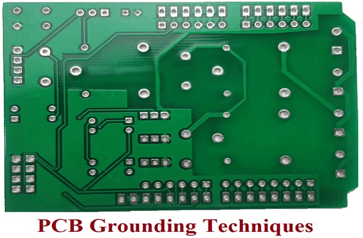
PCB Grounding Techniques that Every Designer Should Know
A proper Grounding is important for any circuit to work as designed, the importance of grounding cannot be stressed enough especially if the circuit consists of many analog and switching components. When designing a Printed Circuit board (PCB) the designer should ensure that all the ground signals are free from noise. There are many grounding methodologies in PCB design that are followed by engineers, the common ones are like including a common ground point, ensuring efficient flow of signals to ground, reducing the use of series vias, etc.. These techniques help us to keep the PCB ground free from the noise. In this article, we will look into all these common ground practices to design PCBs that are free from ground noise.
Common Ground plane
Using a ground plane is the most common technique used by many PCB designers. A ground plane, typically made of copper, covers all the areas of a PCB that do not have components or traces on them. Some rules apply for a ground plane depending on the number of layers a board has. For instance, if your board has two layers, the rules state that you should pace the ground plane on the bottom layer and the traces and components on the top layer.
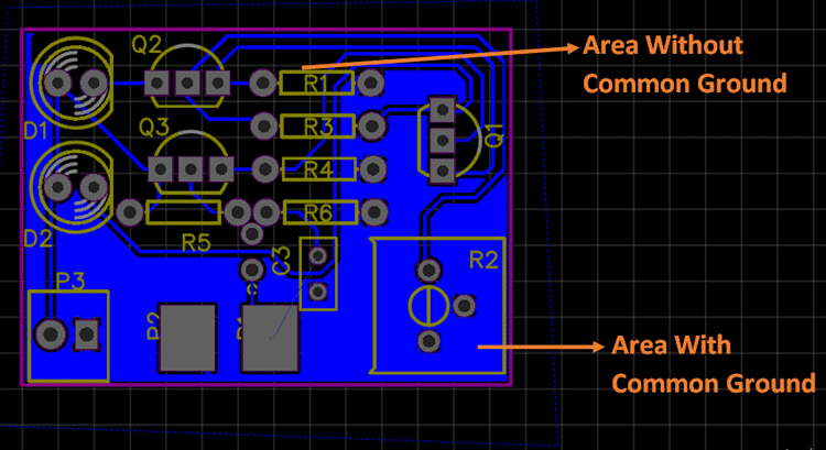
When placing the ground plane, you should ensure that it does not form a ring of conductive material. The ring increases the susceptibility of the ground plane to electromagnetic interference (EMI). When an external magnetic field comes into contact with the conductive ring, it acts as an inductor, causing an electric current known as a ground loop. The ground loop interferes with other circuits generating electrical noise.
When you place a ground plane underneath on the whole bottom layer and remove all parts containing electrical components, a conductive ring may be formed. You should ensure that the traces are as short as possible and place the ground plane under them to prevent the occurrence of the rings. Additionally, you can avoid creating conductive rings by adjusting the layout of traces and components.
Ground plane Vias
In the case you have ground planes on either side of the PCB, the vias are instrumental in establishing a connection between the multiple layers of the multi-layered PCB board. Vias are holes that penetrate the board and connect the two faces of the PCB.
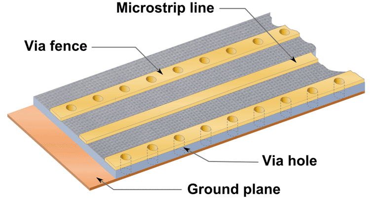
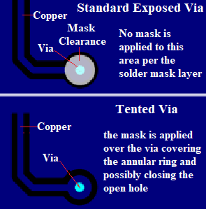
The vias allow you as the designer to have access to the ground plane at any point where it is located. Therefore, providing a conductive path for passing an electrical signal between the multiple layers of the PCB board through plated hole wall. There are various types of vias, but performance is essentially the same. Via should be tented as it minimizes the chances of a short that is synonymous during overflow. Tenting vias is a process in which the vias of a PCB are insulated. Using vias also helps the designer to eliminate ground loops as they directly connect the ground points connected through a low impedance. Besides, it minimizes the length of the return loops.
The ground plane usually resonates at a specific wavelength of the frequency of the current passing into it. You should place the vias at precise intervals around the ground plane to avoid ground planes from resonating. Tented vias are an important aspect of the PCB board as they aid in cooling a hot running component by absorbing heat through the vias to the other side of the board where it can disperse.
In cases where the PCB board layout did not have vias, you can use a small drilling machine to drill several holes. A copper is then passed through the holes and soldered so that a connection on both sides is implemented.
Decoupling
Decoupling is the process of implementing an L-C network next to the integrated circuit chip to provide a transient switching current. Fitting the integrated circuit chips with supply pins links them to an external power supply. Also, they contain ground pins that connect them to the ground plane of the PCB. You should place the decoupling capacitor between the supply pin and the group plane to smooth out oscillation that is generated by the voltage being supplied in the chip.
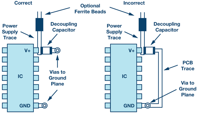
Decoupling capacitors are vital in improving and enhancing the functionality of the PCB. Capacitors are designed to store charge, and thus, the decoupling capacitor in the PCB acts as the charge storage device. Therefore, if there is a demand for more charge by the IC, the decoupling capacitor supplies the charge to the IC through a low inductance path. Apart from enhancing PCB functionality, the decoupling capacitors are effective in reducing noise generated by power supplies on the multi-layered planes. Furthermore, the decoupling capacitor reduces EMI.
However, placement of the decoupling capacitor should be thoroughly considered to maximize n their functionality. You should distribute them across the PCB board with some placed next to or close to the IC ground. Also, the used decoupling capacitor should be of the highest value of capacitance, and all of them should have the same value. You should combine high equivalent series resistance and ordinary capacitors, as a way of maximizing the performance and functionality,
Connector Ground
You must ensure that all the connectors in the PCB linked to the ground and signal lines form a parallel connection. This is attained by separating each connector from the other through the use of a ground pin. PCBs that contain a single connector pin leading to the ground is associated with impedance mismatch, a factor that heavily contributes to oscillations. The oscillations negatively affect the functionality and performance of the PCB.
This means that if there is a fluctuation or elevation of the signal levels, the systems will not perform as designed. Thus the signal levels should remain constant at all times. Therefore, we recommend that you ensure that an S pin leading to the ground.

Latest Articles
-

Single-Sided vs. Double-Sided PCBs: Which One Is Right for Your Project?
-

Exploring the Different Types of PCB Layers and its Purpose
-

PCB Connectors: A Comprehensive Guide to the Different Types and Their Applications
-

PCB Soldering Steps
-

Basic Electronic Component Symbols that Every PCB Design Engineer Should Know
-

Home Made PCBs – A Step by Step guide to build PCBs in your Home
Comments