

Eagle Tutorial 3/4 – PCB Routing and Board Layout in EAGLE
In the previous EAGLE Tutorial, we have learned how to make an EAGLE schematic diagram for any electrical circuit. Now, to continue with our EAGLE PCB Tutorial, we will make an EAGLE PCB layout also known as a board diagram. The schematic diagram of the LED chaser circuit is explained in the previous tutorial. We will continue the same example and make a board diagram.
Board diagram is the most important part of any PCB Design because in this part the designer has to consider the size of PCB, place of the component, and how to connect all components using copper trace. Normally during PCB designing the size of the PCB is kept as small as possible to make the final board compact and cheap.
Schematic to board editor on EAGLE:
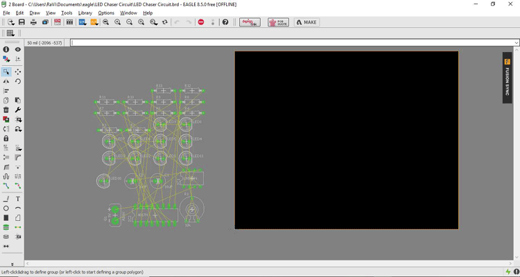
Click the icon (Generate/switch to board) to switch layout.  When you click the first time on this icon, it will ask to generate the board layout in a new window. It looks like the below picture. Once the board diagram is generated, it will directly switch between both layouts.
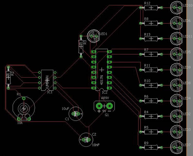
In this new window, you can find the components used in the schematic diagram. These components are placed on the left side of the window. The black space is available on the right side. This place is used to make a board layout. Now place all components in the black space. While placing the component, make sure that connections are not overlapped, provide space for the component and make the proper distance between two neighbor components.
In the above screenshot, the yellow lines are called airwires. The white lines are showing the shape of the component. When you route airwires in EAGLE, it becomes red or blue color. The red and blue color shows the layer of PCB. If PCB is single-sided, use only one color (layer). If PCB is double-sided you can connect component in blue color. When a number of components are more, to avoid overlap and make small size PCB, the double layer is used and, in this case, you can route in both layers.
Arranging components for board layout in EAGLE:
On the left side of the board editor, there is a toolbar. These tools are useful to arrange the components. These tools are similar to the schematic editor. Use the MOVE tool to move a component.  You can also rotate the component while moving by right click. To move the component in the group, select components, click the MOVE tool, hold CTRL and move with the right-click. Use the ROTATE tool to rotate the component.
  When you MOVE the component, use right-click for the rotate the component.
In the board layout, the shape of the component is similar to the shape of the actual component. The designer must consider the white line shown around the component. This line must not overlap in the nearby component.
Routing components in EAGLE:
Routing means turning all yellow lines (airwires) into the top or bottom copper traces. For routing the components, the ROUTE tool is used.  While routing, the designer has to make sure that not to overlap two different signals.
When you select the ROUTE tool, a new toolbar appears as shown in the below screenshot.

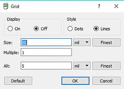
This tool is for the grid. From here, you can ON and OFF the grid. Same as the schematic layout, inboard layout two grid styles are available; dots, and lines.
The designer has to choose the layer of the copper trace.  If PCB is double-sided you can place the component on both sides. For that, you have to choose the copper trace (top or bottom). During routing, airwires for the top layer (1) is converted into red wires and airwires for the bottom layer (16) is converted into the blue wire.
The designer has to place components in a very small place. Hence, the distance between the two components may be small. This creates obstacles while routing the component. In this case, to remove obstacles, there are three tools.
For single-layer PCB bottom layer is not available. So, here you can ON and OFF the single layer. For double layer PCB, OFF the single-layer mode and for single-layer PCB ON the single-layer mode. . There are many turns (curves) in the copper trances. You can choose the shape of these curves.
You can set the width of the copper layer. Use the WIDTH option from the route toolbar to set the width.  The designer has to select the shape of the vias. There are three options to choose from. The shape, diameter, and drill can be set.
RIPUP tool is used to remove the traces.  It is difficult to go back and work again. RIPUP tool is easy to delete the traces. You can also use UNDO and REDO.
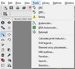
In the paid version of the EAGLE, a great tool is available that is Autorouter. This tool is used to save time for routing. After auto-routing you can change if you need. This tool is not available in the free version of EAGLE.
DRC- Design Rule Check
DRC tool is used to check the board diagram. According to the set of design rules, the DRC tool checks the board layout and shows ERRORS and WARRINGs. If the designer made a mistake in routing, it will highlight the components, which is not connected properly.
Generate Gerber File
Gerber file is a universal file extension for PCB design. For the fabrication of the PCB, the Gerber file is used. You can use any PCB designing software, to design the PCB. But the output is one common file that is Gerber file. Gerber file describes all layers are used in the PCB. For all layers, the Gerber file is different. The below table shows a list of Gerber files with the file extension.
|
Gerber File |
Extension |
|
Top Copper |
.gtl |
|
Bottom Copper |
.gbl |
|
Top Soldermask |
.gts |
|
Bottom Soldermask |
.gbs |
|
Top Silkscreen |
.gto |
|
Bottom Silkscreen |
.gbo |
|
Drill File |
.txt |
|
Drill Station info File |
.dri |
|
Photoplotter info File |
.gpi |
|
Mill Layer |
.gml |
|
Top Paste |
.gtp |

Latest Articles
-

Single-Sided vs. Double-Sided PCBs: Which One Is Right for Your Project?
-

Exploring the Different Types of PCB Layers and its Purpose
-

PCB Connectors: A Comprehensive Guide to the Different Types and Their Applications
-

PCB Soldering Steps
-

Basic Electronic Component Symbols that Every PCB Design Engineer Should Know
-

Home Made PCBs – A Step by Step guide to build PCBs in your Home
Comments