

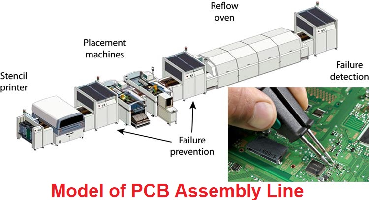
SMT Soldering Process in PCB Assembly Factory
PCBs are found in almost every Electronic device and with the increased demand for Electronic devices all around the world, their production rate is increasing day by day. There are many small and big PCB manufacturers all over the world and all are trying to provide quality services and customer satisfaction to stand out in the competition. Though their services can differ in terms of quality and number but they follow almost the same PCB assembling process to build the PCB. So today we will discuss the PCB assembly process in detail.
Generally, a good PCB manufacturer provides various services like SMT Assembly, BGA Assembly, Through-Hole Assembly, Mixed Assembly, Rigid-Flex PCB Assembly Services, etc. and they are in compliance with a wide range of standard including IPC 610 Class 2 and Class 3.
Process of SMT (Surface-mount Technology) Soldering
Here we divided the complete SMT soldering process into 10 steps:
- Printing
- Adhesive Dispense
- Component Placement
- Pre-Reflow Automated Optical Inspection (AOI)
- Reflow Soldering
- Post-Reflow Automated Optical Inspection (AOI)
- Conformal Coating
- Final Inspection and Functional Test
- Washing & Drying
- Packaging & Shipping
Now we will explain each of the steps in detail.
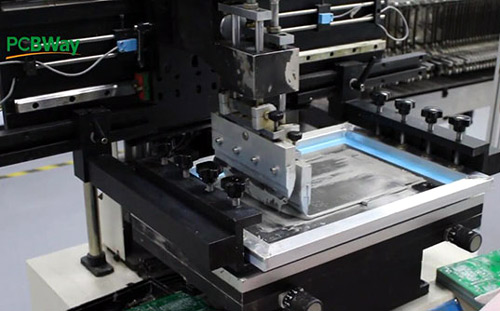
Step 1: Printing:
Printing solder paste on PCB’s solder pad is the first step in the PCB assembling process. It is done by solder paste printing press which is located at the end of the production line to print solder paste or patch adhesive onto PCB's solder pad to prepare components for welding.
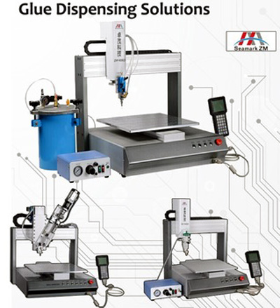
Step 2: Adhesive Dispense:
This process is to use the glue dispenser which is mainly used for precise spot injection of glue paint and other liquids to the precise position of each product to drop the glue on the fixed position of PCB, and its main function is to fix the components to PCB when wave solder is used.
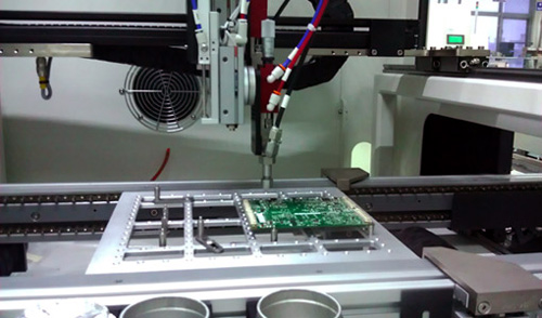
Step 3: Component Placement:
Once the printed PCB has been confirmed to have the correct amount of solder paste applied, it moves into the next part of the manufacturing process which is component placement. Each component is picked from its packaging using either a vacuum or gripper nozzle, checked by the vision system, and placed in the programed location at high speed. There is a large variety of machines available for this process and it depends greatly on the business to what type of machine is selected. For example, if the business is focused around large build quantities, then the placement rate will be important, however, if the focus is a small batch/high mix, then flexibility will be more important.
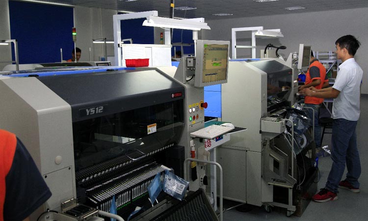
This picture shows the Component Placement Machine PCBWay Assembly factory.
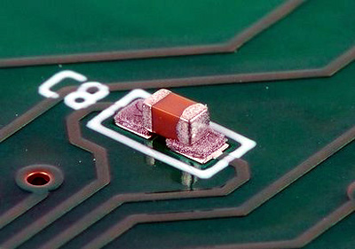
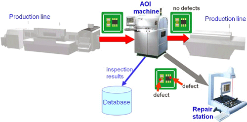
Step 4: Pre-Reflow Automated Optical Inspection (AOI):
It is very vital to take inspection after finishing component placement because whether components are connected correctly or not, as it can influence the whole function of the PCB. The best way of doing this is by using an AOI machine to make checks such as component presence, type/value, and polarity.
Step 5: Reflow Soldering:
Reflow soldering is a process in which a solder paste (a sticky mixture of powdered solder and flux) is used to temporarily attach one or several electrical components to their contact pads, after which the entire assembly is subjected to controlled heat, which melts the solder and permanently connects the joint. Heating may be accomplished by passing the assembly through a reflow oven or under an infrared lamp or by soldering individual joints with a hot air pencil. Reflow soldering is the most common method of attaching surface mount components to a circuit board, although it can also be used for through-hole components by filling the holes with solder paste and inserting the component leads through the paste. Because wave soldering can be simpler and cheaper, reflow is not generally used on pure through-hole boards. When used on boards containing a mix of SMT and THT components, through-hole reflow allows the wave soldering step to be eliminated from the assembly process, potentially reducing assembly costs.

Step 6: Post-Reflow Automated Optical Inspection (AOI):
The last part of the surface mount assembly process is to again check that no mistakes have been made by using an AOI machine to check solder joint quality. Sometimes, the movement during the reflow process will result in poor connection quality or a complete lack of a connection. In other words, shorts are also a common side effect of this movement, as misplaced components can sometimes connect portions of the circuit that should not connect. Thus, the inspection after reflow soldering is quite important and checking for these errors and misalignments can involve one of several different inspection methods. The most common of these inspection methods include the following:
- Manual Checks
- Automatic Optical Inspection(AOI)
- Automated X-ray inspection(AXI)
Step 7: Conformal Coating:
The conformal coating material is a thin polymeric film that ‘conforms’ to the contours of a Printed Circuit Board to protect the board's components. Typically applied at 25-250 μm (micrometers) thickness, it is applied to electronic circuitry to act as protection against moisture, dust, chemicals, and temperature extremes. If uncoated (non-protected), then it could result in damage or failure of the electronics to function. When electronics must withstand harsh environments or impact, protection is provided with conformal coatings or potting compounds. Most circuit board assembly houses coat assemblies with a layer of transparent conformal coating, which is lighter and easier to inspect than potting.
Conformal coating in the PCBWay assembly factory.
Step 8: Final Inspection and Functional Test:
After the soldering and conformal coating steps of the PCB assembly process are finished, a final inspection will test the PCB for its functionality by the Quality Assurance team. This inspection is known as a "functional test". The test software and tools are usually provided by the customer, PCB manufacturers can also make fixtures according to customer requirements. The test puts the PCB through its paces, simulating the normal circumstances in which the PCB will operate. Power and simulated signals run through the PCB in this test while testers monitor the PCB's electrical characteristics.
Step 9: Washing & Drying:
There are oil and dirt in the whole production process, so PCB is cleaned and dried before it goes out. For example, soldering paste leaves behind some amount of flux, while human handling can transfer oils and dirt from fingers and clothing to the surface of the board.
Step 10: Packaging & Shipping:
All assembled boards are packaged (can request in anti-static packaging) and shipped through various courier services like DHL, FedEx, UPS, EMS, and so on. Any unused components are returned in accordance with customer instructions. Additionally, customers are notified via email when their packages ship. Here are the examples:
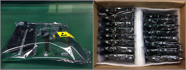
Products assembled at PCBWay
Also, check the below video of the PCBWay Assembly factory to know about the complete process followed in assembling any PCB (Printed Circuit Board).

Latest Articles
-

Single-Sided vs. Double-Sided PCBs: Which One Is Right for Your Project?
-

Exploring the Different Types of PCB Layers and its Purpose
-

PCB Connectors: A Comprehensive Guide to the Different Types and Their Applications
-

PCB Soldering Steps
-

Basic Electronic Component Symbols that Every PCB Design Engineer Should Know
-

Home Made PCBs – A Step by Step guide to build PCBs in your Home
Comments