

Common Mistakes while designing a PCB and Tips to avoid them
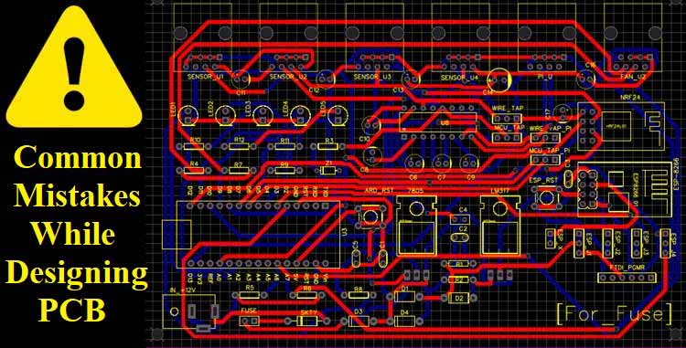
PCBs are normally designed after the complete circuit design is tested and finalized. Once the PCB design is done the design file will be sent to the PCB manufacturer for fabrication. On average these boards will be manufactured in large numbers and after fabrication, if the board has any mistakes, it will end up as a nightmare for the PCB Design engineer, since all the fabricated boards have to be dumped as waste. This is why a PCB Design Engineer needs to make sure that his design does not have any mistakes before he sends it out for fabrication, these mistakes can be made anywhere from the time of choosing the design tool till preparing the final Gerber file for fabrication.
In this article, we will discuss the common mistakes made during PCB designing so that we can watch out for them and make sure we avoid those mistakes in our design. So let’s get started….
Wrong choice of PCB Design Software:
The initial phase of the design process involves the selection of the design software. There are many design tools for PCB, some of which could be inefficient. The inefficient design tools lead to issues such as delayed designing time and increased cost of manufacturing.
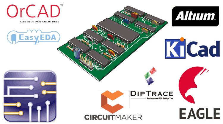
Before settling on a particular design tool, you should conduct a thorough analysis of the design tools to ensure that you select the one that suits the requirements of your PCB. Ease of use should also be considered while choosing the design tool to ensure that a lot of time that would have otherwise be used in the design process is not wasted on learning how to use the tool. If you are confused about selecting the right type of design software, you can read the article on how to choose the best PCB design software which will help you in deciding.
Improper placement of Decoupling Capacitors
Decoupling capacitors allows the product to have a stable power supply. These capacitors are placed on the power supply rail. The decoupling capacitors will not function well if the PCB designer places them incorrectly and far from the pin to which they are supplying power.
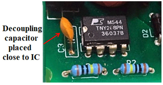
To avoid this mistake, you should ensure that you place them close to the pin that they are supplying power so that they function optimally. Placing the capacitors the correct way and the right distances also improve transient response.
Footprint / Landing Pattern Errors
All PCB design tools provide the designer with the libraries for electric components. The libraries contain the schematic symbol and the landing patterns for the components. There are no mistakes that occur when a designer sticks to the components catered for by the libraries.
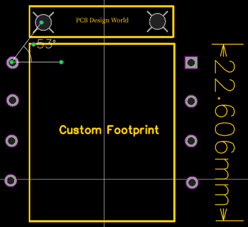
However, the libraries in the PCB design tools are limited as the components keep changing and reducing in size. This makes the designer create own footprints/landing patterns for the PCB when the available libraries cannot suffice. This design process needs high precision and, therefore, increases the probability of errors occurring. For instance, an error of a fraction of a millimeter in the pad-to-pad spacing means that the pins will not align properly, and the soldering process will be difficult, if not impossible. These mistakes are avoided by making that all the measurements are correct.
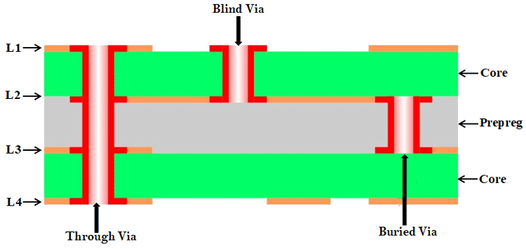
Not sticking to the Via rules
Vias connect different layers of the board. A through via connects all the layers (L1, L2, L3, and L4, as shown in the diagram below) of the board. A blind via connects an external layer to an internal layer of the board. A buried via connects an internal layer to another.
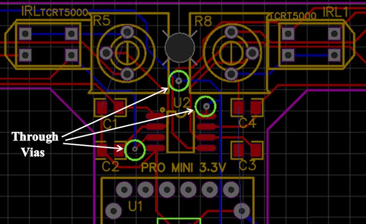
The use of vias should be controlled to ensure that they do not lead to an increase in the size of the board as they reduce the routing space on the layers. The layers not using the vias are also affected. Designers often make the mistake of designing buried or blind vias that are very hard to manufacture or cannot be manufactured at all. Fabricating with buried via or blind vias is a more costly process as compared to a regular through vias, this increases the total cost of the PCB. Additionally, the designer should take into consideration the limitations on which layers the different types of vias can or cannot be used to connect. For instance, a buried via (3) cannot be used to connect layer 1 (L1) to layer 3 (L3).
Inefficient Wireless Antenna Layout
When designing a PCB with wireless functionalities, the designer would often have to design an antenna on the PCB board. This is a delicate process and often mistake occur when the impedance between the transceiver and the antenna is not matched. When this happens, there is no maximum power transfer between the two as required and your antenna will simply not work.
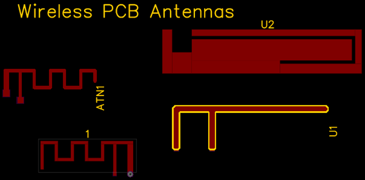
A proper microstrip makes it simple for creating a transmission line in the PCB, it must be used to match the impedance between the antenna and the transceiver. The designer must adequately understand the microstrip transmission line to build one that meets his/her needs. A microstrip designed with an impedance of 50 ohms, in most cases, provides the antenna and the transceiver a maximum power transfer. To achieve this impedance, the designer must set the width of the microstrip based on the dielectric specification of PCB. The designer can use online microstrip calculator tools, most of which are available for free, to get the correct measurements. Also, it is important to ensure with the fabricators that the transceiver and antenna are also installed correctly.
Insufficient width for Power Traces
Some designers tend to use minimum width allowed for a power trace regardless of the amount of current passing through a trace. For instance, for a trace with a current of 500mA, the minimum allowed width would be insufficient.
The width of a trace depends on its location on the external or internal layer, and it's width. The traces on the external layers can carry more current as compared to a trace of the same thickness on the internal layers. The reason for this is because the trace on the external layer can dissipate heat easily to the air.
The width of the traces depends on the thickness of the copper used for that particular layer. The allowed copper thickness/weight varies from 0.5 to 2.5 oz/sq.ft. There are online trace width calculators that designers can use to ensure they use the optimal copper thickness.
Conclusion
The design process of a PCB is marred with the probability of mistakes due to the high precision associated with the process. However, these mistakes are avoidable or can be corrected before the actual fabrication of the PCB. Use of the correct design tools, observing the rules and limitations of every component, and using the correct measurements help in avoiding these mistakes.

Latest Articles
-

Single-Sided vs. Double-Sided PCBs: Which One Is Right for Your Project?
-

Exploring the Different Types of PCB Layers and its Purpose
-

PCB Connectors: A Comprehensive Guide to the Different Types and Their Applications
-

PCB Soldering Steps
-

Basic Electronic Component Symbols that Every PCB Design Engineer Should Know
-

Home Made PCBs – A Step by Step guide to build PCBs in your Home
Comments