

KiCad Tutorial 4/5 – PCB Design and Routing
In the last article, we looked at the development of electronics schematics with Kicad, along with some of the tips and tricks involved with getting the schematics ready for Kicad’s PCBnew software. For this article, we will look at transforming the schematics and netlist generated with Kicad’s EEschema, into PCB using the Kicad PCBnew software.
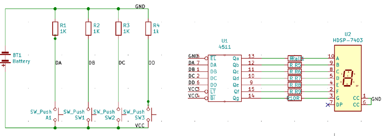
For this tutorial, we will be using the same 7-Segment driver schematics which we created in the previous articles (shown in the image below).
Launch Kicad, and open that project to view all its files. Before we go to the PCB, we need to assign the footprint for components. To do this, click on the EEschema Icon ![]() in the project window. When it opens, click on the “assign footprint to symbol” icon
in the project window. When it opens, click on the “assign footprint to symbol” icon ![]() if all the footprints have been assigned, the center panel of the window should look like mine below.
if all the footprints have been assigned, the center panel of the window should look like mine below.
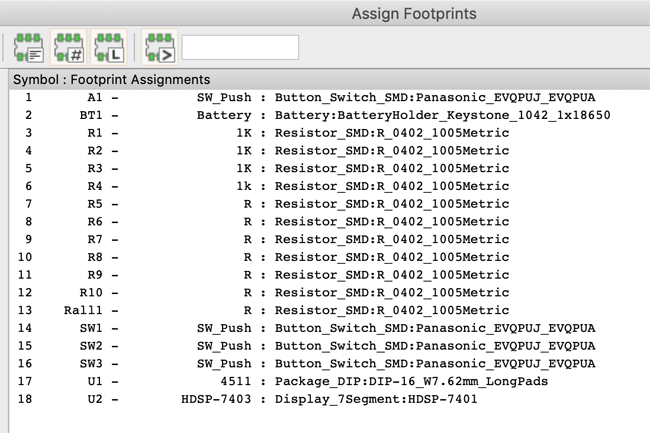
If they have not been assigned, go through the last tutorial which shows how to assign footprints in KiCad and proceed with assigning the footprints such that it looks like the image above.
With the footprints, all assigned, save all, and go back to EEschema. We have to regenerate the netlist so the new changes made to the footprint can reflect. Do this by clicking the net list icon ![]() , select PCBnew as the target, and click on the generate netlist button.
, select PCBnew as the target, and click on the generate netlist button.
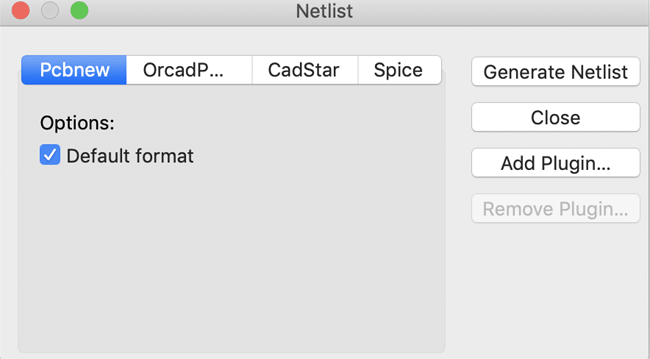
Save it such that it replaces the netlist generated in our previous tutorials.
With this done, we are now ready for the PCB. Click the PCBnew Icon on the top toolbar of the EEschema or go back to the Kicad Project window and click the PCBnew icon. This will launch the PCBnew WIndow. The PCB new windows have almost the same outlook(except for the dark theme) as the EEschema in terms of the way the tools are placed. Tools used in the creation of the PCB itself are found on the right toolbar, while tools used to disable or enable several view options are on the left toolbar. The top toolbar comprises of icons used to perform tasks like zoom, go back to EEschema, change in between layers, etc.
We start just like with the EEschema, by performing the page settings, and entering some information about the PCB. This is done using the Page settings tool. Click on the icon and fill the resulting window as shown below. Click the OK button to implement the changes.
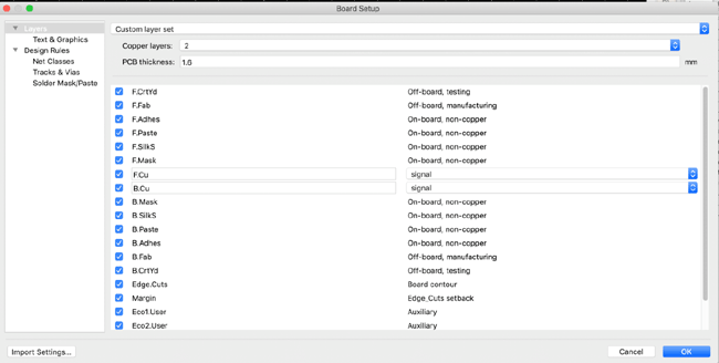
Next, depending on the complexity of your project and how automated you want things to be, it is important to create the design rules for your project. To do this, go to File and click on Board Setup. It should launch a window similar to the image below.
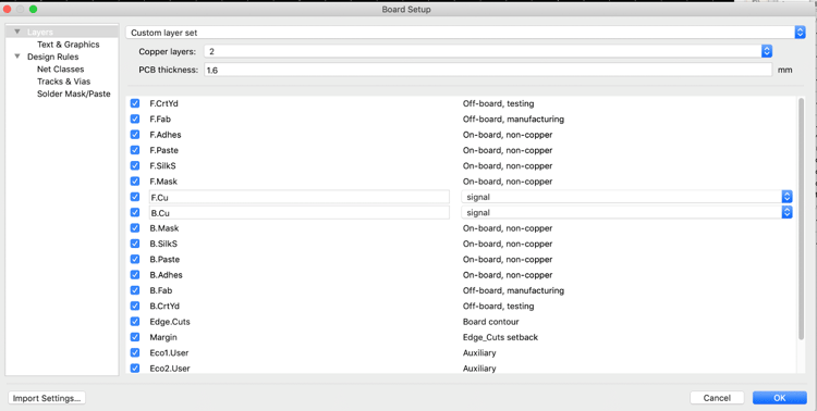
There are two major options under board setup; Layers and Design Rules. Layers allow you to set the number of layers the PCB should have, the thickness of the PCB and the elements of each layer.
The design rules, on the other hand, allow you to set the Net classes. It can be used to create a different type of Nets which could help you easily change between different thicknesses of copper when routing the PCB. It could also help you create nets with different clearance, width, via size, etc all of which simplifies your work when designing the PCB.
Just like the nets, you could also add specialize track widths, via sizes, etc. Lastly the solder mask clearance and width.
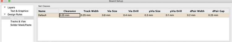
For this tutorial, we will only be setting properties of the default netlist to the minimum requirements of the board manufacturer we will be using. Set the netlist parameters (by clicking on each parameter to edit it) to match the image below and click the Ok button to save the changes.
With all setup done, we are now ready to import the netlist and start designing the PCB. As mentioned during the introduction, the netlist is how the EEschema interacts with the PCBnew. Thus to pass all the design information created on EEschema to PCBnew, the netlist has to be imported.
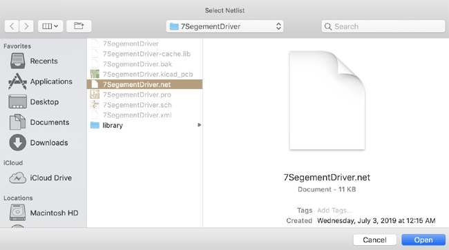
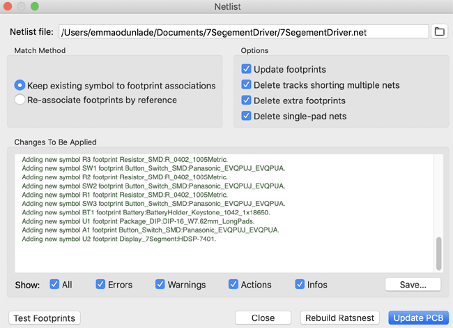
Import the netlist by clicking the “Load netlist” ![]() icon. This will open a window with space for you to enter the directory for the netlist file and a small button for you to navigate to the project folder where the netlist file is saved.
icon. This will open a window with space for you to enter the directory for the netlist file and a small button for you to navigate to the project folder where the netlist file is saved.
Click on the button, and it should automatically take you to the project file currently opened in Kicad. The netlist file (with .net extension) will be the only file active in the folder.
Select it and click ok, the directory should now be loaded on the window. The window also has options on the integration and appearance of the netlist but for now, stick to the default configuration and click the “Update PCB” button. Followed by the close button.
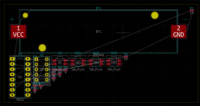
With this done, your canvass should now look like the image below with all the components loaded. Do note that you might need to adjust your zoom percentage to see things properly.
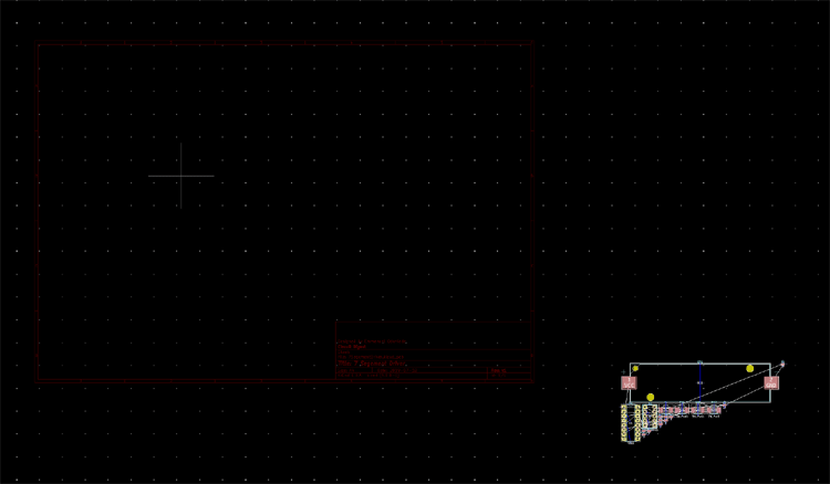
You can now use the move hotkey to move all the components within the Sheet we created (bounded by red).
At this point, all the components are connected by thin wires called rat nest.
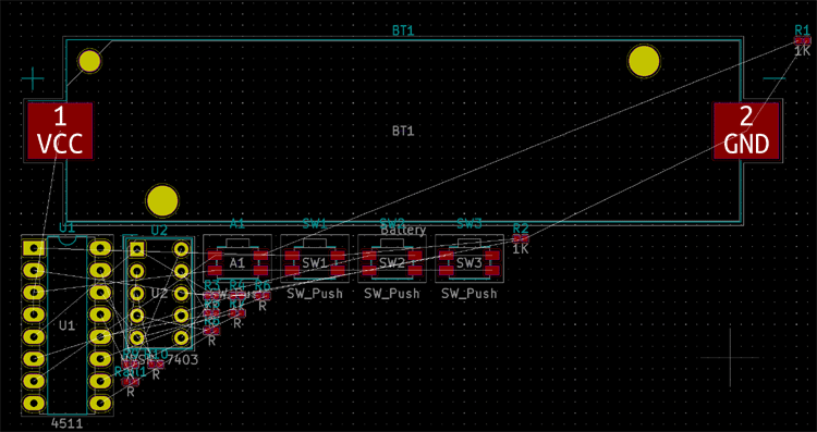
While the netlist import process tries to help with the arrangement of the components, as shown above, there may be a need for you to move the components around. This can be done with move hotkey “m”. Other actions like rotate etc can also be done using their hotkeys. You can check the list of all the hotkeys available under PCBnew by going to “help” on the top toolbar and selecting “list hotkeys”.
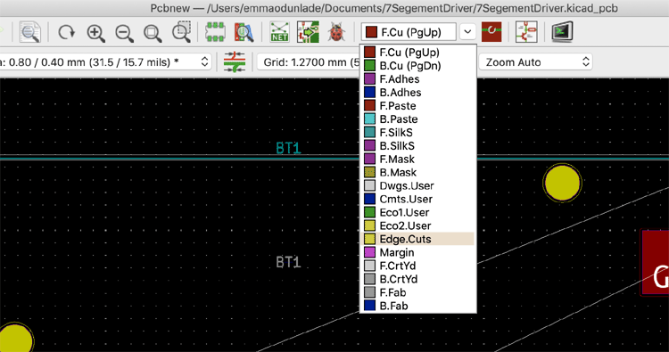
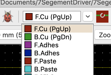
With all the components positioned as desired, We now proceed to draw an edge for the PCB. Start by changing the focus of the layers dropdown on the top toolbar to edge.cuts as shown below.
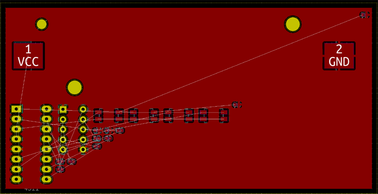
Next, click on the “add graphics line” icon, select a starting point for the edge demarcation and drag around the board, by clicking at remaining edges (ensuring that there is enough space between the components and the line) such that a rectangle is formed. There should now be a yellow line drawn around the components as shown below.
For boards which are not a straight-up rectangle like above, maybe as a result of the kind of enclosure to be used and other factors, you can use the other graphics icons like the “add graphics arc” and the “add graphic circle” icons combined with the add graphics line icon to create your board edge.
With the board edge created, we can now begin to route the tracks. There are two ways to route your board in kicad;
- Use of Auto Routers like Free Router
- Manual Routing
To pick them one after the other;
1. Use of Auto Routers like Free Router
Auto routers use design rules to automatically route the PCB board.
When to use auto routers is usually a thing of preference. Some prefer it when the board is not complex as they believe more attention is needed for complex boards, while others use it to reduce the workload associated with the design of complex boards. A balance is however attained in the design of complex boards by routing the critical components by hand and deploying the autorouter for the rest.
Several autorouter software exists for kicad, but most of them are a modified version of a free router as such we will be using a free router for this article.
FreeRouter is an open-source application for routing PCBs. It allows users to import their PCB designs from EDA software and routes the board based on predefined design rule, routing only the unrouted traces. A procedure for downloading a free router is available here.
To use a free router, with board edge created and critical traces routed(if necessary), On PCBnew, click File -> Export -> Spectral DSN and save the file.
Next launch free router, select the “open your design button” browse for the DSN file you just saved and launch it.
Start the routing process by clicking on the auto-router button on the top bar. You may need to spread your components out the more or rotate some of them to reduce the number of rat nests crossing one another. Once the job is done, click on File and select Export Spectra Session File. This will export the routed file.
You can then go back to PCBnew and import the routed board by going to File - > Import - > Spectra Session, and delete any trace you don’t like, reroute it, and proceed to finalize your board design.
2. Manual Routing
This, on the other hand, involves routing the board within the Kicad PCBnew window.
With the edge of the board defined, one of the first steps to reduce the amount of work to be done is to create a GND plane that will route all pins connected to ground, all at once.
To do this, start by deciding which side of the board you want the ground plane to be. For this tutorial, we will be creating it on the Top/front copper (side) of the PCB. Change the dropdown at the top toolbar to reflect Top copper.
Then click on the “add filled zones” icon on the right toolbar and use it to trace a rectangle around the board, just like we did for the board edge. As soon as you click the first corner with the tool selected, it will launch a dialog box like the one in the image below, allowing you to set the properties of the copper filled zones. The key properties include the Layer (on which the zone is to be created), the net, which in this case will be the GND net(all pins connected to gnd) and the constrains. The dialog box also allows you to set things like the pad clearance, width of the trace, track clearance among other factors. Set these parameters as shown in the image below and select ok.
![]()
With this done, move the cursor around the board, clicking at the edges till you get back to the point where you started from. The board should now look like the image below.
All the nets labeled GND will now be connected to the ground plane. To continue the routing of the remaining rat nest, you can disable the top copper so you can see the components properly. Do this by unchecking the top copper box under the layer manager, beside the right toolbar or by clicking the “Do not Show Filled Areas” ![]() Icon on the left toolbar.
Icon on the left toolbar.
Next, Connect the rest of the traces. Do this by selecting the copper layer (choose whichever one works for the particular rat nests) and then use the Route Track tool to join the rat nests one after the other. Due to the SMD nature of the switch and resistors used in the schematics, they must be connected to the top copper, but as you continue the route, you might get to a point where that will no longer be possible as the routes will have to cross one another with the alternative is going through routes that you may dim too long. It is at this point that you make use of vias.
Using Vias in KiCad
Vias help you route traces in between two or more layers. It allows you to change the copper plane while you are running a trace.
To do this on kicad, While you are running a trace, right-click at the point where you want to add the via and select “place through via”. You can see the color change as the copper plane changes as illustrated below.
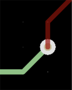
Vias can be very useful when navigating through a crowded board.
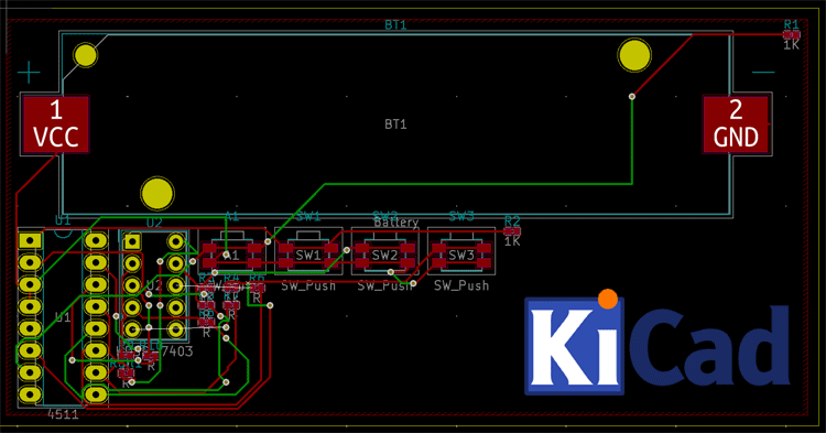
Route tracks through all the ratnests such that the board now looks like the image below. Too many visas? Yes, let’s just go with it for the sake of this tutorial.
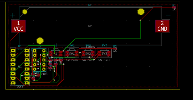
Activating the filled zones, using the “show filled zones” icon, gives the board the look below.
PCB Design Rule Check
To ensure everything is as it should be and that there are no errors in the board design, you will need to run the board design rule checker. This is done by clicking on the “Design Rules Check” ![]() Icon. This will launch the DRC Control window. Click on the Run DRC button, It may generate some errors showing unconnected pins like the image below.
Icon. This will launch the DRC Control window. Click on the Run DRC button, It may generate some errors showing unconnected pins like the image below.
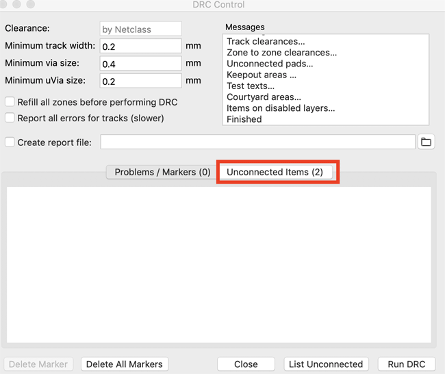
Make efforts to connect those pins then run the check again till you have zero unconnected pins.
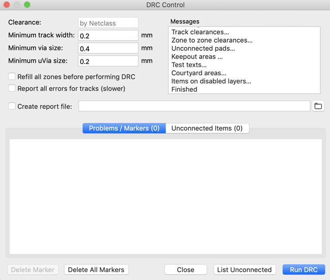
With this done, the board is officially ready.
Add Text to the PCB Layout
To do things the right way, at this point, you could also add text to indicate the board type, version, and other information that could help with the maintenance of the board going forward.
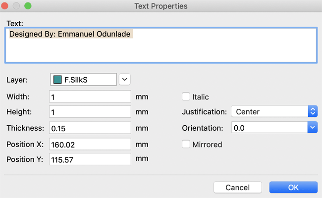
To add text to the board, set the layer at the top toolbar to F.silks (Top Silk) and click on the “add text” icon on the right toolbar. This will launch a window for you to enter the text to be displayed and edit its font size, thickness amongst others. Enter the text you desire and click Ok.
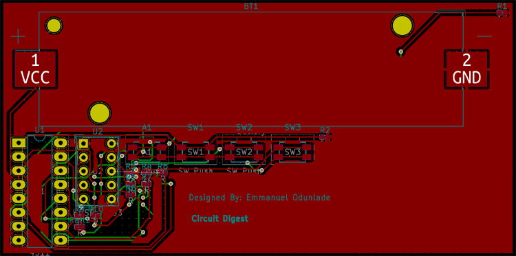
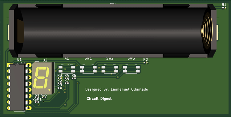
Your Board should now look like the image below with the text on it.
Before we go to CAM and generate the Gerber files, one of the good things about Kicad is, it provides you an opportunity to view your board in 3D, giving you an idea of what it will look like when manufacturing is done.
3D view on KiCad
To view your board in 3D, go to view at the top of the page and select 3D viewer. This should open a window with your board displayed like the image below.
With this done, Your PCB is ready and we can now generate the Gerber files.
Generating the Gerber Files
While still within the PCBnew window, go to File and select the plot. This will launch a window that will allow you to select the layers of the board and other features of the Gerber files that should be generated.
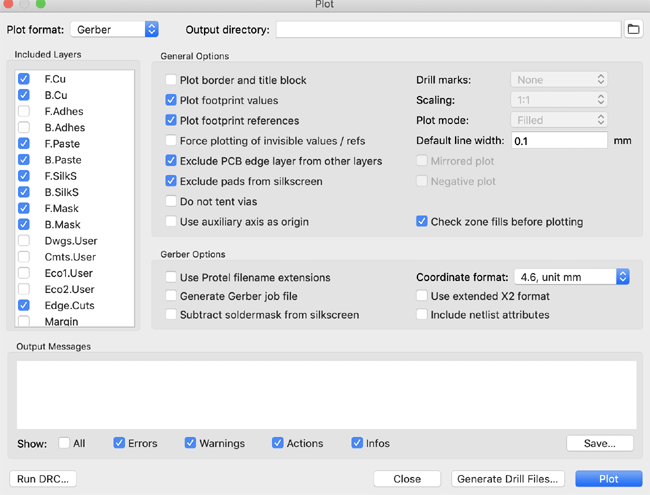
For a typical two-layer board, the default settings should be fine. Click on Plot. The Gerber files will now be generated and saved into the same folder as the PCB.
This file can now be sent to your favorite board house to fabricate the PCB.
Most PCB houses will run DRC checks on your board and let you know if there is an error before they proceed with manufacturing while some won’t. As such, it is important to double-check your designs before shipping them off for manufacturing.
That’s it for this article, thanks again for reading. The next one will cover tips and tricks for the Kicad PCBnew, in addition to things like creating your symbol footprint and viewing Gerber files with Kicad. Till Next time.

Latest Articles
-

Single-Sided vs. Double-Sided PCBs: Which One Is Right for Your Project?
-

Exploring the Different Types of PCB Layers and its Purpose
-

PCB Connectors: A Comprehensive Guide to the Different Types and Their Applications
-

PCB Soldering Steps
-

Basic Electronic Component Symbols that Every PCB Design Engineer Should Know
-

Home Made PCBs – A Step by Step guide to build PCBs in your Home
Comments