

PCB Track Width and Track Resistance – Importance, Calculation, and Design Tips
PCB boards are the basic element of all the electronic devices that we are using today. These PCB boards are used to minimize the size and complications that are involved in the wired circuits. The wires in typical circuits are converted as tracks in a PCB. Just like a wire, these tracks also have their own resistance and the maximum current that flow through it depends on its width. Further the width and resistance of the track also decides the voltage drop across the track. So, it is very important for a PCB Designer to calculate the right width and Resistance of his tracks.
If you are completely new to PCB, then it is highly recommended for you to read this PCB Basics article before you proceed any further.
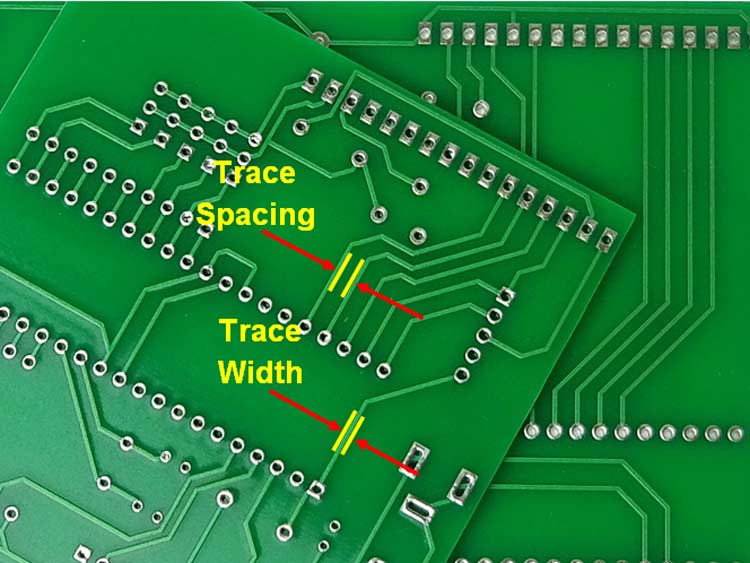
What is a PCB Track or PCB Trace?
A Track on a PCB is a conductive path or the running path of copper that runs all over the circuit board, they act as a connection between two points on the PCB. The conductive path will be connecting two different components in the PCB and the PCB Tracks are also sometimes referred to as a PCB Trace. These tracks are used to spread signal and power to each and every component on the PCB. One should always keep an eye on the PCB Track Width and resistance because they ensure effective operation in transmitting signal and power and provides optimal operation of the PCB.
Factors to consider while designing a PCB track
There are certain factors that are considered before designing the PCB Track such as Purpose, Amperage, Location, Thickness, and length. These factors help in improving the operation of the PCB board in a suitable way for any particular application.
Purpose: The purpose defines what kind of parameter does the track is going to carry, whether the Track is a power track or the Signal track. Power tracks should always be wider than the signal track. The actual width can be calculated by using formulae which we will discuss later.
Amperage: The design of the track also depends on the amount of the current that the track is going to carry. When the current pass through the track, it will generate heat, the track should be wide enough to handle the heat.
Location: There will be a lot of components included on the circuit board which will be connected with one another with different tracks, these tracks should not be too close to each other as they will lead to the risk of shorting and burning of the circuit board
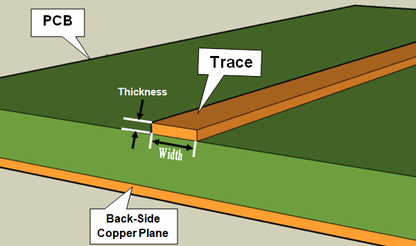
Thickness: The thickness of the copper track and the Width of the track is directly related to one another. These two factors decide the maximum current carrying capability of the track.
Length: The length also plays a major role in the designing of the PCB Track because the length should not affect the efficiency of the current flow. If you want a lot of power for your circuit you should have longer tracks.
If the above pointers are not taken into consideration the circuit might not work as expected. Using the wrong track width is one of the common mistakes made by PCB designers. If you are interested, you can read about the other common mistakes that might occur during PCB design to make sure you avoid it during your design process.
PCB Trace width Calculation:
Now that we know the things to consider while drawing a PCB track, let’s learn how to calculate the optimum width for a PCB track. Today, PCB Design software themselves provides an option for you to calculate the PCB trace width and trace resistance, put in this article lets learn about the actual formulae behind it.
As defined by the IPC standards under IPC 2221, the formula for the allowable current passing through the track can be given as
I=k*ΔT^0.44*A^0.725
Where I stand for current and it will be considered as a constant value. ΔT stands for the change in temperature and A represents the cross-sectional area of the Track. If you want to derive the track width from the above formula you should rearrange the formula to find the cross-sectional area for the chosen current to pass through the Track. The re-arranged formula will look like the following
Area[mils^2] = (Current[Amps]/(k*(Temp_Rise[deg. C])^ 0.44))^(1/0.725)
Once you have found out the area of the track it will be easy to calculate the width of PCB track by considering the thickness of the track with the help of the following formula
Width[mils] = Area[mils^2]/(Thickness[oz]*1.378[mils/oz])
These derivatives of formulas can be used for the tracks that carry current from 0 to 35 ampere, in which the temperature might rise from 10°C to 100°C.
PCB Track Design Tips
The Track width of the PCB always depends on the design specifications and the amount of current you want to pass through the tracks, for the track width there is a general rule of thumb that has been followed in most of the application.
As per the general rule of thumb, the minimum Route Track Width is 1.0mm/A. The track width is applicable for 1.0oz/ft2 of copper thickness, which is the common thickness of the copper used in most of the PCBs. Although this track width is commonly used there are some exceptional cases for special applications where this rule isn’t followed, in such cases, you can use the PCB track width calculators.
PCB Track resistance and its importance
The copper is the most preferred metal for designing the PCB track due to its least resistive character when compared with other metals. In PCB designing the resistance of the track is considered as the most important factor which needs to be calculated and analyzed during the designing of the PCB as it might affect the overall performance of the PCB. Knowing the Resistance of the track will help you to understand how much power a track can take and how fast it can transmit communication signals along the PCB.
PCB Trace Resistance Calculation
Unlike the Track width, calculation of copper trace resistance has been just as simple as applying the ohms law if you know the required parameters. The PCBs are designed with the help of the PCB suits and development environment that has an inbuilt PCB track resistance calculator.
The PCB track resistance is calculated with the help of the following formula
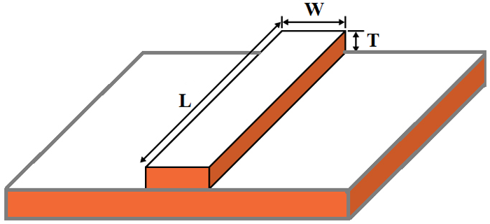
R = r . (L/T . W) [1 + α . (temp – 25)]
Where L, W, and T represent the physical parameters like Length, Width, and Thickness of the Track, represents the resistivity of the material used, in most of the cases, copper and represents the temperature coefficient of the copper. The calculation helps to determine the approximate resistance of the track, it cannot be more accurate because it is hard to find the exact resistance of the material without physically testing it.
When we talk about the Track Resistance, we cannot neglect the power loss caused by track resistance. If the device is a small signal PCB, there might not be much power loss in it, which can be neglected in most cases. But in the case of a power circuit, there will be a huge loss even if there is a slight change in the resistance, If there is a loss in power, it will lead to a rise in temperature and a reduction in conductivity. To avoid these complications and to compensate for the Track Resistance, the PCB track area is increased. The resistance of the track should be appropriate to maintain the efficient operation of the PCB board.

Latest Articles
-

Single-Sided vs. Double-Sided PCBs: Which One Is Right for Your Project?
-

Exploring the Different Types of PCB Layers and its Purpose
-

PCB Connectors: A Comprehensive Guide to the Different Types and Their Applications
-

PCB Soldering Steps
-

Basic Electronic Component Symbols that Every PCB Design Engineer Should Know
-

Home Made PCBs – A Step by Step guide to build PCBs in your Home
Comments